Testing SATA Express And Why We Need Faster SSDs
by Kristian Vättö on March 13, 2014 7:00 AM EST- Posted in
- Storage
- SSDs
- Asus
- SATA
- SATA Express
During the hard drive era, the Serial ATA International Organization (SATA-IO) had no problems keeping up with the bandwidth requirements. The performance increases that new hard drives provided were always quite moderate because ultimately the speed of the hard drive was limited by its platter density and spindle speed. Given that increasing the spindle speed wasn't really a viable option for mainstream drives due to power and noise issues, increasing the platter density was left as the only source of performance improvement. Increasing density is always a tough job and it's rare that we see any sudden breakthroughs, which is why density increases have only given us small speed bumps every once in a while. Even most of today's hard drives can't fully saturate the SATA 1.5Gbps link, so it's obvious that the SATA-IO didn't have much to worry about. However, that all changed when SSDs stepped into the game.
SSDs no longer relied on rotational media for storage but used NAND, a form of non-volatile storage, instead. With NAND the performance was no longer dictated by the laws of rotational physics because we were dealing with all solid-state storage, which introduced dramatically lower latencies and opened the door for much higher throughputs, putting pressure on SATA-IO to increase the interface bandwidth. To illustrate how fast NAND really is, let's do a little calculation.
It takes 115 microseconds to read 16KB (one page) from IMFT's 20nm 128Gbit NAND. That works out to be roughly 140MB/s of throughput per die. In a 256GB SSD you would have sixteen of these, which works out to over 2.2GB/s. That's about four times the maximum bandwidth of SATA 6Gbps. This is all theoretical of course—it's one thing to dump data into a register but transferring it over an interface requires more work. However, the NAND interfaces have also caught up in the last couple of years and we are now looking at up to 400MB/s per channel (both ONFI 3.x and Toggle-Mode 2.0). With most client platforms being 8-channel designs, the potential NAND-to-controller bandwidth is up to 3.2GB/s, meaning it's no longer a bottleneck.
Given the speed of NAND, it's not a surprise that the SATA interface quickly became a bottleneck. When Intel finally integrated SATA 6Gbps into its chipsets in early 2011, SandForce immediately came out with its SF-2000 series controllers and said, "Hey, we are already maxing out SATA 6Gbps; give us something faster!" The SATA-IO went back to the drawing board and realized that upping the SATA interface to 12Gbps would require several years of development and the cost of such rapid development would end up being very high. Another major issue was power; increasing the SATA protocol to 12Gbps would have meant a noticeable increase in power consumption, which is never good.
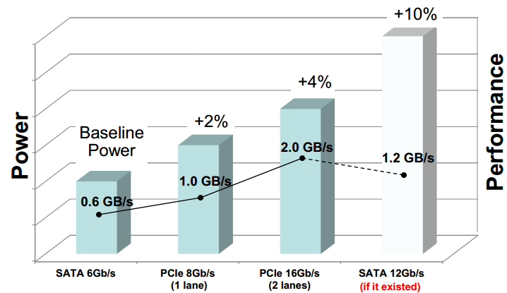
Therefore the SATA-IO had to look elsewhere in order to provide a fast yet cost efficient standard in a timely matter. Due to these restrictions, it was best to look at already existing interfaces, more specifically PCI Express, to speed up the time to the market as well as cut costs.
| Serial ATA | PCI Express | |||
| 2.0 | 3.0 | 2.0 | 3.0 | |
| Link Speed | 3Gbps | 6Gbps |
8Gbps (x2) 16Gbps (x4) |
16Gbps (x2) 32Gbps (x4) |
| Effective Data Rate | ~275MBps | ~560MBps |
~780MBps ~1560MBps |
~1560MBps ~3120MBps (?) |
PCI Express makes a ton of sense. It's already integrated into all major platforms and thanks to scalability it offers the room for future bandwidth increases when needed. In fact, PCIe is already widely used in the high-end enterprise SSD market because the SATA/SAS interface was never enough to satisfy the enterprise performance needs in the first place.
Even a PCIe 2.0 x2 link offers about a 40% increase in maximum throughput over SATA 6Gbps. Like most interfaces, PCIe 2.0 isn't 100% efficient and based on our internal tests the bandwidth efficiency is around 78-79%, so in the real world you should expect to get ~780MB/s out of a PCIe 2.0 x2 link, but remember that SATA 6Gbps isn't 100% either (around 515MB/s is the typical maximum we see). The currently available PCIe SSD controller designs are all 2.0 based but we should start to see some PCIe 3.0 drives next year. We don't have efficiency numbers for 3.0 yet but I would expect to see nearly twice the bandwidth of 2.0, making +1GB/s a norm.
But what exactly is SATA Express? Hop on to next page to read more!


131 Comments
View All Comments
SunLord - Thursday, March 13, 2014 - link
I like the idea but they should of rolled there own custom connector not twist the sata connector to meet there needs it's looks stupid. A custom high density connector and cable designed specifically for its task would make far more sense then this hodgepodge but I guess they need to cut comers to "keep costs down" on something already aimed at the high end which is even stupider. A nice clean high density interface with an sata adpater would of been far better.androticus - Thursday, March 13, 2014 - link
Ugh. What an immensely cumbersome and kludgy design.asuglax - Thursday, March 13, 2014 - link
Kristian, I completely agree with your final thoughts. I would actually take it a step further and say that Intel should completely do away with the DMI interface and corresponding PCH; they should limit the I/O off the processor to as many as possible PCI-e lanes, 3 DisplayPort (which can be exposed as dual-mode), and however many memory channels. Enterprise could have QPI, additionally. I would like to see I/O controllers embedded into the physical interconnects where PCI-e could be routed to the interconnects and however many USB, SATA, or other connections could be switched and exposed through the devices (I supposed it could be argued that this could be a PCH in itself, only connected through PCI-e instead of DMI). Security protection measures (such as TPM's functionality) should be built-in to all components and, while being independently operative, be able to communicate with one-another through the presented I/O channels.fteoath64 - Saturday, March 15, 2014 - link
@asuglax: Intel is known and has done this. Provide small incremental adds to the processor and chipset features so they can provide as many iterations of SKUs as they can over a period of time. If they do a radical change, then they risk not being able to manage the incremental changes they wanted. It is a strategy to allows for a large variety of product units, hence expanding the market for themselves. Lately, you see that they have reduced the number of CPU skus while expanded the mobile mobile skus. This is possible since in both market segments they are the majority leader and allows them to maximise profits with minimal changes to production. It is a different strategy for AMD and a completely different one yet for the Arm SoC vendors. Intel's strategy seems like it is coercing the market to move to a place and pace they wanted. The Arm guys just give their best shot on every product they have so we got a lot more than we paid for.You just cannot teach an old dog new tricks.
Babar Javied - Thursday, March 13, 2014 - link
This SATA 3.2 really doesn't make a lot of sense to me and others also seem to agree from when I've read in the comments. Is this supposed to be a temporary thing or the middle man before we get to the good stuff? like SATA 4.0, is that the reason why it's called SATA 3.2?So here is a genuine question. Why not just use Thunderbolt? It is owned by intel and they can implement it into their next chipset(s). Also, Thunderbolt uses PCIe lanes so it is plenty fast without wasting lanes. Sure, the controller and cables are expensive but once it starts to be mass produced they should come down as is common with electronics.
It seems to me that SATA is going though a lot of trouble to bring 3.2 when it is only marginally better. I also get the feeling that SSDs are going to get even faster by using more channels (current standard is 8) and NAND chips (current standard is 16) as they become the new standard in storage. Of course the transition from HDD to SDD is not going to happen overnight but it is going to happen and I get the feeling that the 750MB/s is going to become a bottleneck very quickly.
And finally, by switching to Thunderbolt, we also help kickstart the adoption of this standard and hopefully see it flourish. Allowing us to daisy chain monitors, storage drives (SSDs and HDDs), external graphic cards and so much more.
SirKnobsworth - Thursday, March 13, 2014 - link
There's no point to implementing Thunderbolt internally, which is what SATAe is for. For external purposes you can already buy Thunderbolt SSDs.SittingBull - Thursday, March 13, 2014 - link
I don't feel like you have proven that there is any need for these faster hard drive interfaces, as you hoped to in the title of your article. The need for, let alone the desire for, higher resolution video is anything but proven by anyone that I know of. 4k video offers only dubious benefits, as only very large displays can show the difference between it and 1080p, ie., 70 or 80 inches! The wider colour gamut would be nice but is not really compelling, and those are the only benefits I am aware of. I seriously doubt that the TV or electronics industry are going to be able to sell the 4k idea to the public as a whole. Even 720p is not shown to be lacking until we get into displays larger than 50 inches.It is always nice to read up on the tech of the future and I thank you for explaining the SATAe and other interfaces that are in the works. Eventually these advances will be implemented but I can't see it happening until there is some sort of substantial demand, and your entire article is built on the premise that we will need the bandwidth to support 4k video quite soon. But we don't ... :(
BMNify - Sunday, March 16, 2014 - link
SittingBull , perhaps you should stick your head out of the Native American Law Students offices and look to your alumni of the Indian Institute of Science for inspiration in the tech world today,given that its clear and public knowledge that the NHK/ BBC R&D years of UHD development http://www.bbc.co.uk/rd/blog/2013/06/defining-the-... and now ratified by the International Telecommunication Union are the minimum base for any new Soc design to adhere to and comply with IF they want to actually reuse their current UHD IP for the longest time scales...
the main point is if the PR are not trying to cover up by acts of omission the fact they don't actually comply with the new Rec. 2020 real colour space is better colour coverage due to using 10bits per pixel for UHD-1 consumer grade panels and later UHD-2 12bit grade panels for the 8192×4320 [8K] consumer in 4 years or so.
to put it simply, antiquated Rec. 709 (HDTV and below) 8bit pseudocolor color = only 256 bands of usable colour.
Rec. 2020 real colour space 10bits per pixel= 1000+ bands of usable colour so you get far less banding in lower bit rate encodes/decodes and more compression for a given bit rate so a better higher visual quality at smaller size.
as it happens, NHK announced they are to give another UHD-2/8K 3840 pixels wide by 2160 pixels high Broadcast Demo at the coming NAB Show,"Japanese public broadcaster NHK is planning to give a demonstration of "8K" resolution content over at single 6MHz bandwidth UHF TV channel at the National Association of Broadcasters (NAB) Show coming up in Las Vegas, Nevada, April 5 to 10."
In order to transmit the 8K signal, whose raw data requirement is 16 times greater than an HDTV signal, it was necessary to deploy additional technologies These include ultra multi-level orthogonal frequency domain multiplex (OFDM) transmission and dual–polarized multiple input multiple output (MIMO) antennas. This was in addition to image data compression. The broadcast uses 4096-point QAM modulation and MPEG-4 AVC H.264 video coding.
we could also have a debate about how qualcomm and other cortex vendors might finally provide the needed UHD-2 data throughput and far lower power with ether integrated JEDEC Wide IO2 25.6GBps/51.2GBps or Hybrid Memory Cube 2.5D interposer-based architectures,and using MRAM inline computation etc.
did you notice how the ARM SoC with its current NoC (network On Chip) can already beat today's QPI real life data throughput (1Tb/s,2Tb/s etc) at far lower power,never mind the slower MCI as above, they only need to bring that NoC capability to the external interconnect to take advantage of it in any number of IO ports
Popskalius - Friday, March 14, 2014 - link
I haven't even taken my Asus z87 Plus out of its shrink wrap and it's becoming obsolete.SittingBull - Friday, March 14, 2014 - link
I just put together my own system with an Asus Z87 Plus mb, an i7 4770k, 16 GB of RAM and an SSD. It is not and will not be obsolete anytime in the near future, ie., at least 3 years. Worry not. There isn't anything on the horizon our systems won't be able to deal with.