NVIDIA Tegra K1 Preview & Architecture Analysis
by Brian Klug & Anand Lal Shimpi on January 6, 2014 6:31 AM ESTTegra K1 ISP & Video
NVIDIA’s Tegra K1 SoC also makes some dramatic improvements on the ISP side. We saw SoCs start arriving with two ISPs sometime in 2013, which allowed OEMs to deliver a host of new imaging experiences, like shot in shot video and simultaneous use of both front and rear cameras. With Tegra K1, NVIDIA is not only moving to two ISPs, but it’s also making ISP more of a first class citizen.
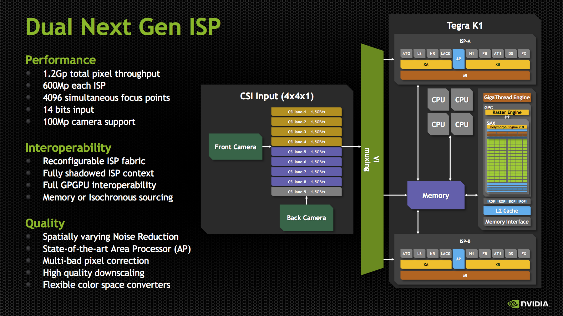
For those not familiar, ISP (Image Signal Processor) handles the imaging pipeline for still photos, video, and performs tasks like Bayer to RGB conversion (demosaicing), 3A (Autofocus, Auto Exposure, Auto white balance), noise reduction, lens correction, and so on. Although NVIDIA has always included an ISP onboard, I couldn’t shake the feeling that still imaging performance could’ve been better, especially in the few cases that allowed direct comparison (HTC One X). With Tegra K1, there’s more die area dedicated to ISP than in the past, and there are two of them to support the kind of dual camera applications that have quickly become popular.
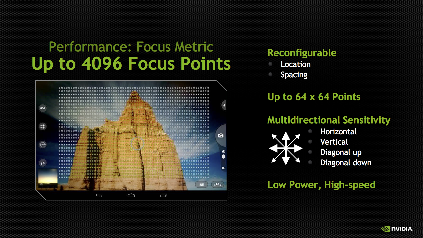
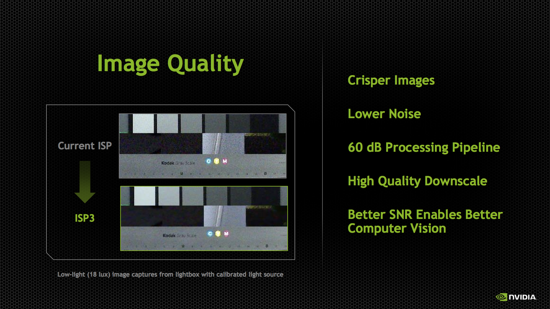
Tegra K1 includes the third generation of NVIDIA’s ISP, capable of processing 600 MP/s on each ISP with 14 bit input, and support for up to 100 MP cameras. There are two of them, so NVIDIA quotes the total pixel throughput as up to 1.2 Gp/s. This is dramatically increased from Tegra 4, which supported up to 400 Mp/s at 10 bits per pixel. In addition the K1’s ISP now supports up to 4096 focus points, a 64x64 array, for its autofocus routine. The ISP also has better noise reduction, and local tone mapping, a feature we’ve also seen become popular for combining parts of images and recovering some of the dynamic range lost with ever shrinking pixel sizes.
Tegra K1 retains compatibility with the Chimera 1.0 features that we just saw in the Tegra Note 7, like object tracking, always-on HDR, slow motion capture, and full resolution burst, and adds more. NVIDIA has kept the Chimera brand for the K1 SoC, calling it Chimera 2.0, and envisions this architecture enabling things like better temporal pixel binning (combining 8 exposures from the CMOS to drive noise down further), faster panorama, video stabilization, and even better live preview with effects applied. The high level of Chimera seems to be the same – kernels that either run on the CPU, or on the GPU (ostensibly in CUDA this time) before or after the ISP and in a variety of image spaces (Bayer or RGB depending).
On the video side, Tegra K1 continues to support 2160p30 (4K or UHD video at 30FPS) encode and decode. Broken down another way, H.264 High Profile Level 5.1 decode and 4K H.264 High Profile 4.2 encode. The fact that there’s a Kepler next door made me suspect that NVENC was used for most of these tasks, but it turns out that NVIDIA still has discrete blocks for video encode of H.264, VP8, VC1, and others. These are the same video encode and decode blocks as what were used in Tegra 4, but with some further optimizations for power and efficiency. The Tegra K1 platform includes support for H.265 video decode as well, but this isn’t accelerated fully in hardware, rather the decode is split across NVENC and CPU.
NVIDIA showed off a K1 reference board doing 4Kp30 H.264 decode on an attached display, I didn’t notice any dropped frames. Of course that’s a given considering we saw the same thing on Tegra 4, but it’s still worth noting that the SoC is capable of driving 4K/UHD displays over eDP 1.4, LVDS and HDMI 1.4b.
The full GPIO breakdown for Tegra K1 includes essentially all the requisite connectivity you’d expect for a mobile SoC. For USB there’s 3 USB 2.0 ports, and 2 USB 3.0 ports. For storage Tegra K1 supports eMMC up to version 4.5.1, and there’s PCIe x4 which can be configured


88 Comments
View All Comments
HighTech4US - Monday, January 6, 2014 - link
You quoting CharLIE and using his Nvidia hate filled speculative drivel as somehow being gospel taints your article.MrSpadge - Monday, January 6, 2014 - link
He is right, occasionally - you've got to give him that. The problem is you never know before it happens, which makes reading the Inq pretty pointless.HighTech4US - Wednesday, January 8, 2014 - link
A broken clock is right twice a day and wrong the rest of the time which is pretty much charLIE's track record on Nvidia.OreoCookie - Monday, January 6, 2014 - link
If you're familiar the style of The Register and The Inquirer (at least in the past when I was reading them regularly), they often packaged excellent tech reporting in their quirky and snarky way of writing things. (I read both back in the day to learn more about the inner workings of cpu designs and such.) (Charlie Demerjian hails from The Inquirer.) And Anand did not treat Demerjian as gospel, he said that it looks as if he may have been spot on.Xavierx78 - Monday, January 6, 2014 - link
Would really like to see the K1 in the next version of OUYA!silenceisgolden - Monday, January 6, 2014 - link
I'm noticing a lack of talk about LTE/radio support stillfafa1971 - Monday, January 6, 2014 - link
They can bundle a discrete modem, NVIDIA i500 (LTE cat. 4, 150 Mbps):http://www.nvidia.com/object/i500-cellular-modems-...
Rayb - Monday, January 6, 2014 - link
Apparently Nvidia decided to avoid the US market for lack of CDMA. It has been certified for AT&T and will be marketed globally, just not in the US because Verizon/Sprint don't use the GSM baseband.http://www.fiercewireless.com/story/nvidia-not-tar...
Krysto - Monday, January 6, 2014 - link
Decent showing from Nvidia with K1, but the real game-changer will be K2, or whatever the hell they'll call it then, with Denver and Maxwell by default, and made at 16nm FinFET. Hopefully it will arrive no later than early spring next year.Normally that chip should get 700 Gflops, but if they can push another 3x, to 1 TF, that would really give them a lot of buzzwords in the media: "Denver", "Maxwell", "16nm FinFET", "1 Teraflops", etc
I hope they don't blow it. Qualcomm is already getting lazy because they have too much domination in the market. We need another strong competitor.
ddriver - Monday, January 6, 2014 - link
Got to love Shang Tsungs' marketing, K1 - the 192 core chip, now coming with either 2 or 4 cores.