Intel Iris Pro 5200 Graphics Review: Core i7-4950HQ Tested
by Anand Lal Shimpi on June 1, 2013 10:01 AM ESTThe Core i7-4950HQ Mobile CRB
At a high level, Iris Pro 5200 would seem to solve both problems that plagued Intel graphics in the past: a lack of GPU hardware and a lack of memory bandwidth. As a mostly mobile-focused design, and one whose launch partner isn’t keen on giving out early samples, it seemed almost impossible to evaluate Iris Pro in time for the Haswell launch. That was until a week ago when this showed up:
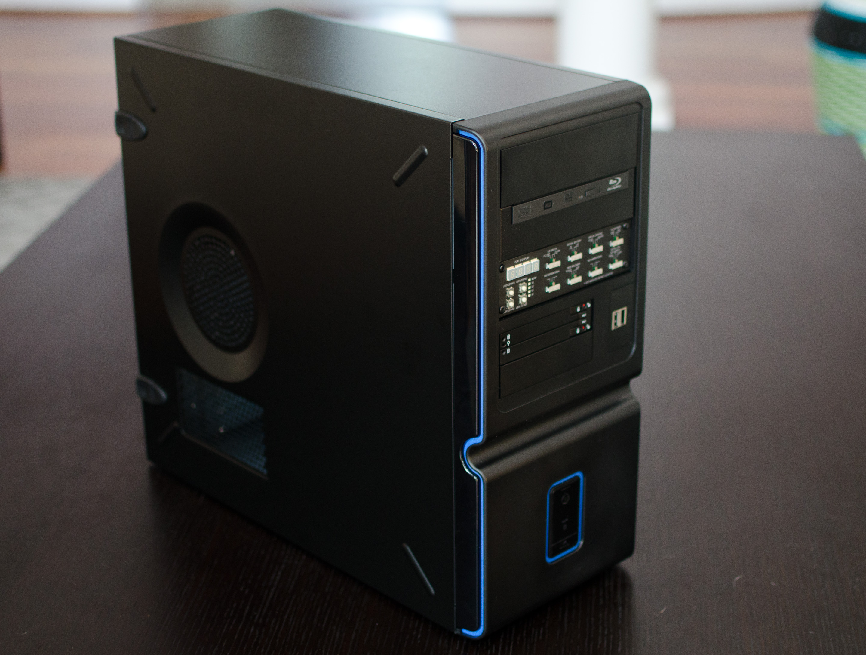
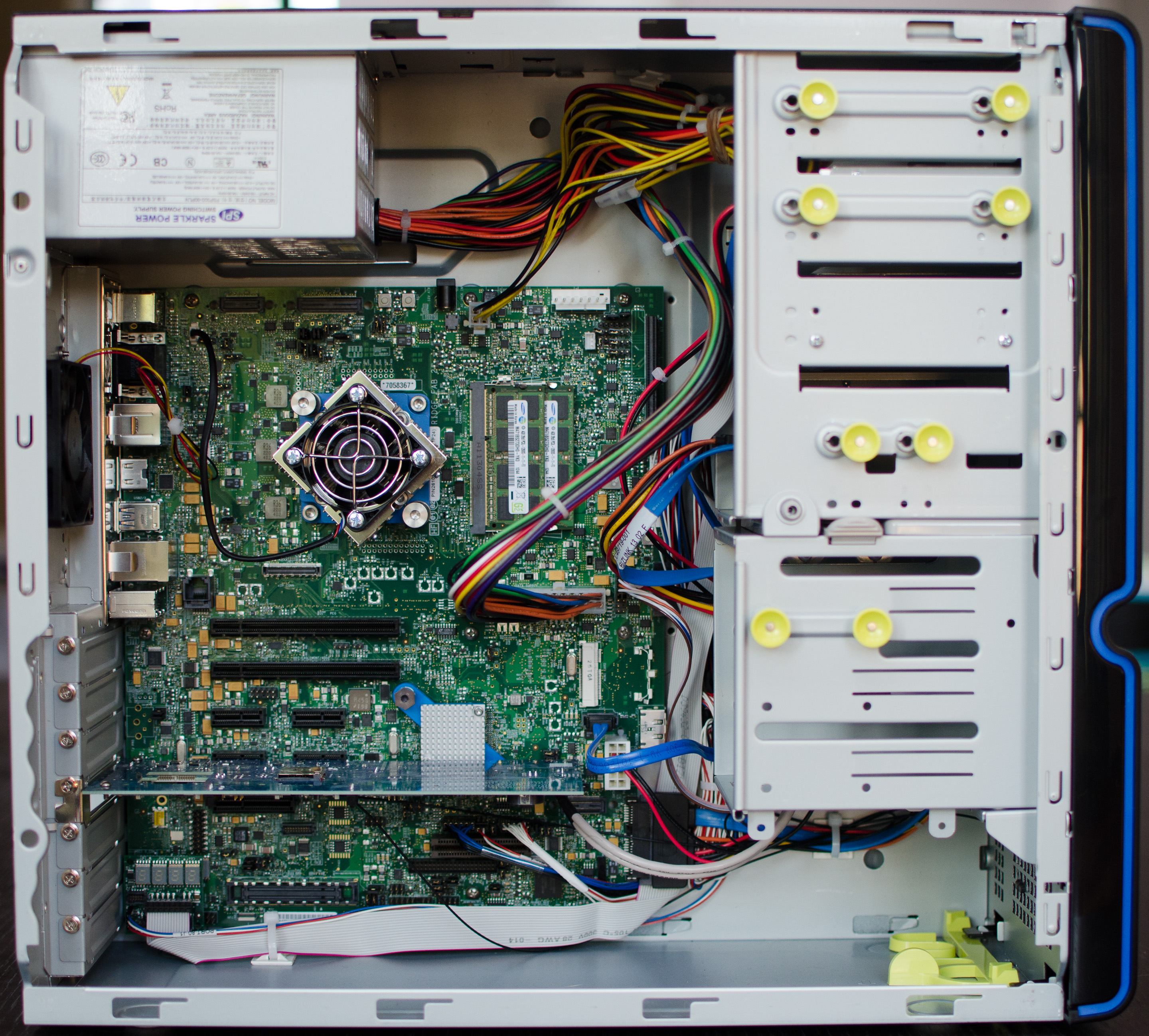
What may look like a funny mid-tower from a few years ago is actually home to one of Intel’s mobile Customer Reference Boards (CRB). Although the chassis is desktop-sized, everything inside is optimized for mobile. It’s just easier to build things larger, especially when it comes to testing and diagnosing problems.
The silicon on-board is a 47W Core i7-4950HQ, the lowest end launch SKU with Iris Pro 5200 graphics. The chassis is obviously overkill for a 47W part, but the performance we get with this machine should be representative of any i7-4950HQ system with a cooler capable of dissipating 47W.
If you read our Haswell CPU review you’ll know that Intel tried to be stingy with telling us die sizes and transistor counts for the bulk of the Haswell lineup, electing to only give us data on dual-core Haswell GT3 and quad-core Haswell GT2. Knowing that mobile parts ship without integrated heat spreaders, I went to work on pulling off the i7-4950HQ’s heatsink (after I finished testing, just in case).
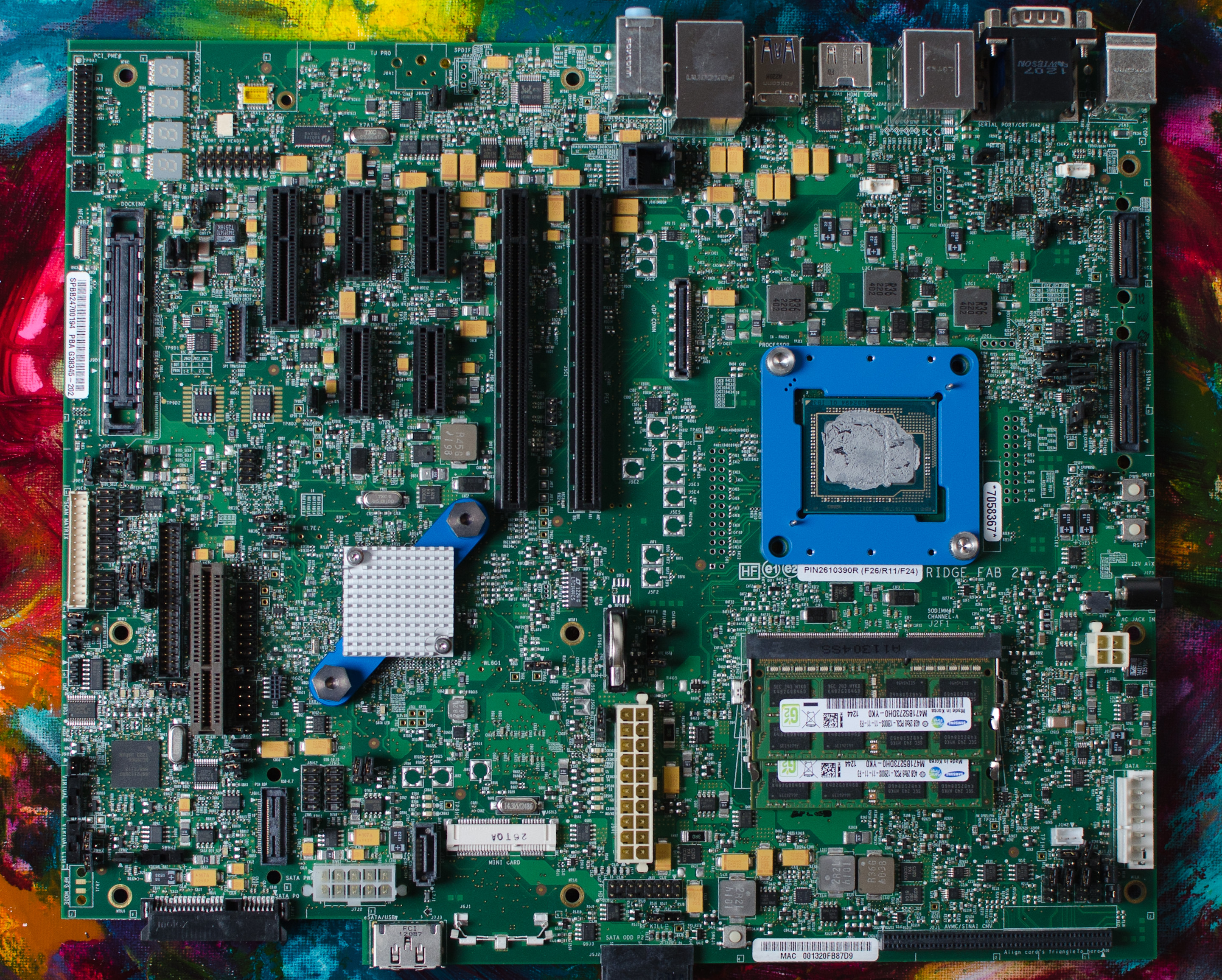
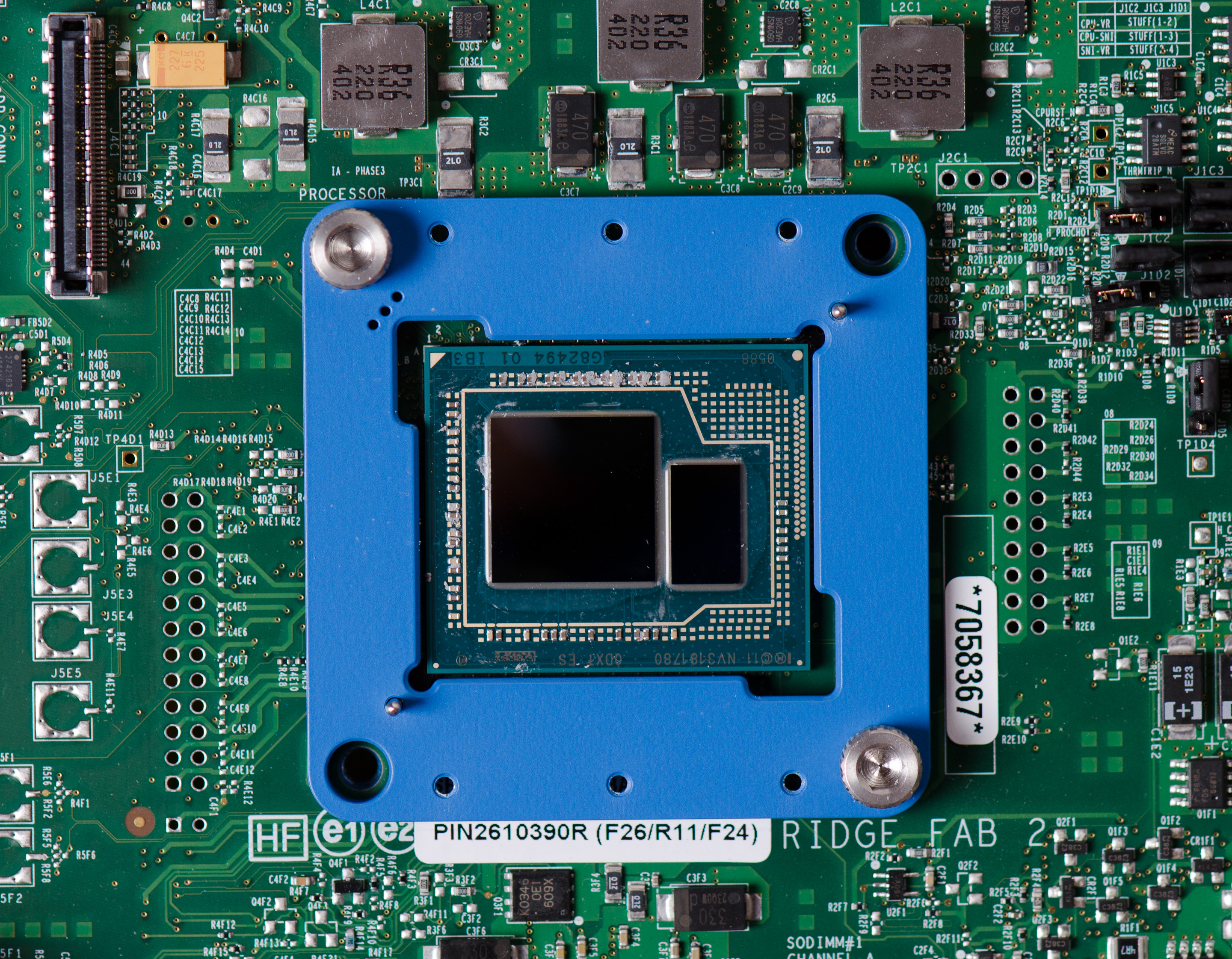
With the heatsink off and thermal paste wiped off, I used my bargain basement calipers to get a rough idea of die area. This is what I came up with:
| Intel Haswell | |||||||||||||||||
| CPU Configuration | GPU Configuration | Die Size | Transistor Count | ||||||||||||||
| Haswell GT3e (QC) | Quad-Core | GT3e | 264mm2 + 84mm2 | ? | |||||||||||||
| Haswell GT2 (QC) | Quad-Core | GT2 | 177mm2 | 1.4B | |||||||||||||
| Haswell ULT GT3 | Dual-Core | GT3 | 181mm2 | 1.3B | |||||||||||||
The Crystalwell die measures 7mm x 12mm (84mm^2), while the quad-core Haswell + GT3 die is a whopping 264mm^2 (16.2mm x 16.3mm). Working backwards from the official data Intel provided (177mm^2 for quad-core GT2), I came up with an 87mm^2 adder for the extra hardware in Haswell GT3 vs. GT2. Doubling that 87mm^2 we get a rough idea of how big the full 40 EU Haswell GPU might be: 174mm^2. If my math is right, this means that in a quad-core Haswell GT3 die, around 65% of the die area is GPU. This is contrary to the ~33% in a quad-core Haswell GT2. I suspect a dual-core + GT3 design is at least half GPU.


177 Comments
View All Comments
boe - Monday, June 3, 2013 - link
As soon as intel CPUs have video performance that exceeds NVidia and AMD flagship video cards I'll get excited. Until then I think of them as something to be disabled on workstations and to be tolerated on laptops that don't have better GPUs on board.MySchizoBuddy - Monday, June 3, 2013 - link
So Intel just took the OpenCL crown. Never thought this day would come.prophet001 - Monday, June 3, 2013 - link
I have no idea whether or not any of this article is factually accurate.However, the first page was a treat to read. Very well written.
:)
Teemo2013 - Monday, June 3, 2013 - link
Great success by Intel.4600 is near GT630 and HD4650 (much better than 6450 which sells for $15 at newegg)
5200 is better than GT640 and HD 6670 (currently sells like $50 at newegg)
Intel's intergrated used to be worthless comparing with discret cards. It slowly catches up during the past 3 years, and now 5200 is beating a $50 card. Can't wait for next year!
Hopefully this will finally push AMD and Nvidia to come up with meaningful upgrade to their low level product lines.
Cloakstar - Monday, June 3, 2013 - link
A quick check for my own sanity:Did you configure the A10-5800K with 4 sticks of RAM in bank+channel interleave mode, or did you leave it memory bandwidth starved with 2 sticks or locked in bank interleave mode?
The numbers look about right for 2 sticks, and if that is the case, it would leave Trinity at about 60% of its actual graphics performance.
I find it hard to believe that the 5800K is about a quarter the performace per watt of the 4950HQ in graphics, even with the massive, server-crushing cache.
andrerocha - Monday, June 3, 2013 - link
is this new cpu faster than the 4770k? it sure cost more?zodiacfml - Monday, June 3, 2013 - link
impressive but one has to take advantage of the compute/quick sync performance to justify the increase in price over the HD 4600ickibar1234 - Tuesday, June 4, 2013 - link
Well, my Asus G50VT laptop is officially obsolete! A Nvidia 512MB GDDR3 9800gs is completely pwned by this integrated GPU, and, the CPU is about 50-65% faster clock for clock to the last generation Core 2 Duo Penryn chips. Sure, my X9100 can overclock stably to 3.5GHZ but this one can get close even if all cores are fully taxed.Can't wait to see what the Broadwell die shrink brings, maybe a 6-core with Iris or a higher clocked 4-core?
I too see that dual core versions of mobile Haswell with this integrated GPU would be beneficial. Could go into small 4.5 pounds laptops.
AMD.....WTH are you going to do.
zodiacfml - Tuesday, June 4, 2013 - link
AMD has to create a Crystalwell of their own. I never thought Intel could beat them to it since their integrated GPUs always has needed bandwidth ever since.Spunjji - Tuesday, June 4, 2013 - link
They also need to find a way past their manufacturing process disadvantage, which may not be possible at all. We're comparing 22nm Apples to 32/28nm Pears here; it's a relevant comparison because those are the realities of the marketplace, but it's worth bearing in mind when comparing architecture efficiencies.