Intel’s Silvermont Architecture Revealed: Getting Serious About Mobile
by Anand Lal Shimpi on May 6, 2013 1:00 PM EST- Posted in
- CPUs
- Intel
- Silvermont
- SoCs
The Silvermont Module and Caches
Like AMD’s Bobcat and Jaguar designs, Silvermont is modular. The default Silvermont building block is a two-core/two-thread design. Each core is equally capable and there’s no shared execution hardware. Silvermont supports up to 8-core configurations by placing multiple modules in an SoC.
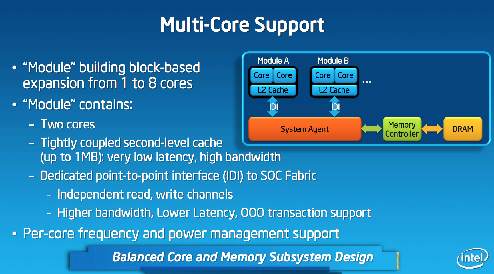
Each module features a shared 1MB L2 cache, a 2x increase over the core:cache ratio of existing Atom based processors. Despite the larger L2, access latency is reduced by 2 clocks. The default module size gives you clear indication as to where Intel saw Silvermont being most useful. At the time of its inception, I doubt Intel anticipated such a quick shift to quad-core smartphones otherwise it might’ve considered a larger default module size.
L1 cache sizes/latencies haven’t changed. Each Silvermont core features a 32KB L1 data cache and 24KB L1 instruction cache.
Silvermont Supports Independent Core Frequencies: Vindication for Qualcomm?
In all Intel Core based microprocessors, all cores are tied to the same frequency - those that aren’t in use are simply shut off (power gated) to save power. Qualcomm’s multi-core architecture has always supported independent frequency planes for all CPUs in the SoC, something that Intel has always insisted was a bad idea. In a strange turn of events, Intel joins Qualcomm in offering the ability to run each core in a Silvermont module at its own independent frequency. You could have one Silvermont core running at 2.4GHz and another one running at 1.2GHz. Unlike Qualcomm’s implementation, Silvermont’s independent frequency planes are optional. In a split frequency case, the shared L2 cache always runs at the higher of the two frequencies. Intel believes the flexibility might be useful in some low cost Silvermont implementations where the OS actively uses core pinning to keep threads parked on specific cores. I doubt we’ll see this on most tablet or smartphone implementations of the design.
From FSB to IDI
Atom and all of its derivatives have a nasty secret: they never really got any latency benefits from integrating a memory controller on die. The first implementation of Atom was a 3-chip solution, with the memory controller contained within the North Bridge. The CPU talked to the North Bridge via a low power Front Side Bus implementation. This setup should sound familiar to anyone who remembers Intel architectures from the late 90s up to the mid 2000s. In pursuit of integration, Intel eventually brought the memory controller and graphics onto a single die. Historically, bringing the memory controller onto the same die as the CPU came with a nice reduction in access latency - unfortunately Atom never enjoyed this. The reasoning? Atom never ditched the FSB interface.
Even though Atom integrated a memory controller, the design logically looked like it did before. Integration only saved Intel space and power, it never granted it any performance. I suspect Intel did this to keep costs down. I noticed the problem years ago but completely forgot about it since it’s been so long. Thankfully, with Silvermont the FSB interface is completely gone.
Silvermont instead integrates the same in-die interconnect (IDI) that is used in the big Core based processors. Intel’s IDI is a lightweight point to point interface that’s far lower overhead than the old FSB architecture. The move to IDI and the changes to the system fabric are enough to improve single threaded performance by low double digits. The gains are even bigger in heavily threaded scenarios.
Another benefit of moving away from a very old FSB to IDI is increased flexibility in how Silvermont can clock up/down. Previously there were fixed FSB:CPU ratios that had to be maintained at all times, which meant the FSB had to be lowered significantly when the CPU was running at very low frequencies. In Silvermont, the IDI and CPU frequencies are largely decoupled - enabling good bandwidth out of the cores even at low frequency levels.
The System Agent
Silvermont gains an updated system agent (read: North Bridge) that’s much better at allowing access to main memory. In all previous generation Atom architectures, virtually all memory accesses had to happen in-order (Clover Trail had some minor OoO improvements here). Silvermont’s system agent now allows reordering of memory requests coming in from all consumers/producers (e.g. CPU cores, GPU, etc...) to optimize for performance and quality of service (e.g. ensuring graphics demands on memory can regularly pre-empt CPU requests when necessary).


174 Comments
View All Comments
GTRagnarok - Monday, May 6, 2013 - link
We'll miss you :'(Pheesh - Monday, May 6, 2013 - link
I don't think the Anandtech site will miss your views and contributions. I appreciated the article and explanations for what's to come. Not everyone cares only about 'specs'.Krysto - Monday, May 6, 2013 - link
That's what I hate most about Intel's press releases, too. They are typically HIGHLY misleading, in some way or another. Remember when they made people believe the 22nm IVB would be 37% faster AND 40% more efficient? - when it was actually one OR the other, but because of the way they phrased it in the PR...and the way tech sites cloned it in their articles, that's what most people got - that they get BOTH those benefits. In the end it was HALF of each.But the worst part about it is the "churnalism" that comes after it. Since most tech sites are either too ignorant or too lazy, they just rewrite what Intel said in the PR - no questions asked.
Please remember EXACTLY what Intel says Silvermont is capable of - and I PROMISE you when this chip gets reviewed, it won't even seem close, and if you remember everything, you'll be disappointed.
Khato - Monday, May 6, 2013 - link
Actually, I don't recall where Intel stating that IVB would be 37% faster AND 40% more efficient. I believe you're confusing technical information regarding the 22nm process capabilities with a product using that process... and incorrectly interpreting that process information to boot.Homeles - Monday, May 6, 2013 - link
The only thing that I can think of is the chart comparing voltage and gate delay on the first page of this article, which was circulating a lot before the launch of Ivy Bridge. There's nothing misleading about it though, unless you don't know how to read the chart.Homeles - Monday, May 6, 2013 - link
"That's what I hate most about Intel's press releases, too. They are typically HIGHLY misleading, in some way or another."Intel, AMD and Nvidia are all guilty of this, and you know it.
t.s. - Tuesday, May 7, 2013 - link
Exactly! Hate it. It looks like all of them have an inferiority complex. They have to boast. Not confident enough with their true offerings.AssBall - Monday, May 6, 2013 - link
You know I have been coming here for 15 years and thought exactly the same thing. This article is the worst. Terrible PowerPoint graphs and gibberish. No real information. Kind of a sadness.VivekGowri - Monday, May 6, 2013 - link
The "PowerPoint" graph actually came from Excel, but it came from an article from earlier this year: http://www.anandtech.com/show/6536/arm-vs-x86-the-... (see page 3). And I dare you to find a more thorough or more comprehensively researched and tested article on SoC power consumption literally anywhere else.AssBall - Tuesday, May 7, 2013 - link
I dared, "literally", but couldn't find much. Sue us for asking for better standards.