Intel's Haswell Architecture Analyzed: Building a New PC and a New Intel
by Anand Lal Shimpi on October 5, 2012 2:45 AM ESTHaswell's GPU
Although Intel provided a good amount of detail on the CPU enhancements to Haswell, the graphics discussion at IDF was fairly limited. That being said, there's still some to talk about here.
Haswell builds on the same fundamental GPU architecture we saw in Ivy Bridge. We won't see a dramatic redesign/re-plumbing of the graphics hardware until Broadwell in 2014 (that one is going to be a big one).
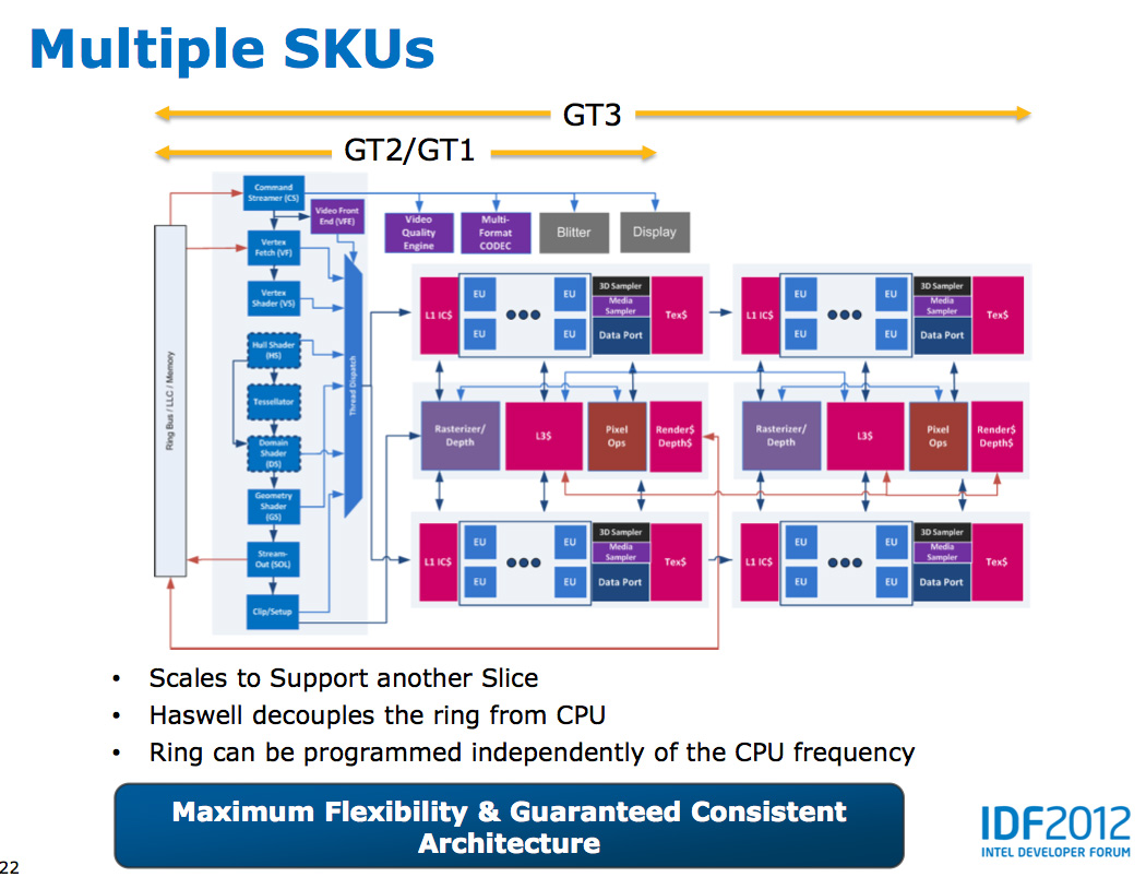
Haswell's GPU will be available in three physical configurations: GT1, GT2 and GT3. Although Intel mentioned that the Haswell GT3 config would have twice the shader count of Haswell GT2, it was careful not to disclose the total number of EUs in any of the versions. Based on the information we have at this point, GT3 should be a 40 EU configuration while GT2 should feature 20 EUs. Intel will also be including up to one redundant EU to deal with the case where there's a defect in an EU in the array. This isn't an uncommon practice, but it does indicate just how much of the die will be dedicated to graphics in Haswell. The larger of an area the GPU covers, the greater the likelihood that you'll see unrecoverable defects in the GPU. Redundancy at the EU level is one way of mitigating that problem.
Haswell's processor graphics extends API support to DirectX 11.1, OpenCL 1.2 and OpenGL 4.0.
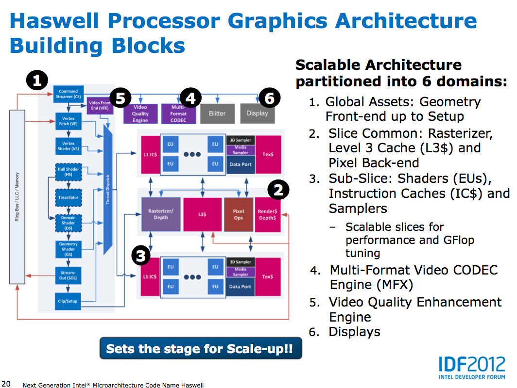
At the front of the graphics pipeline is a new resource streamer. The RS offloads some driver work that the CPU would normally handle and moves it to GPU hardware instead. Both AMD and NVIDIA have significant command processors so this doesn't appear to be an Intel advantage although the devil is in the (unshared) details. The point from Intel's perspective is that any amount of processing it can shift away from general purpose CPU hardware and onto the GPU can save power (CPU cores go to sleep while the RS/CS do their job).
Beyond the resource streamer, most of the fixed function graphics hardware sees a doubling of performance in Haswell.
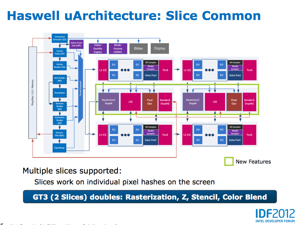
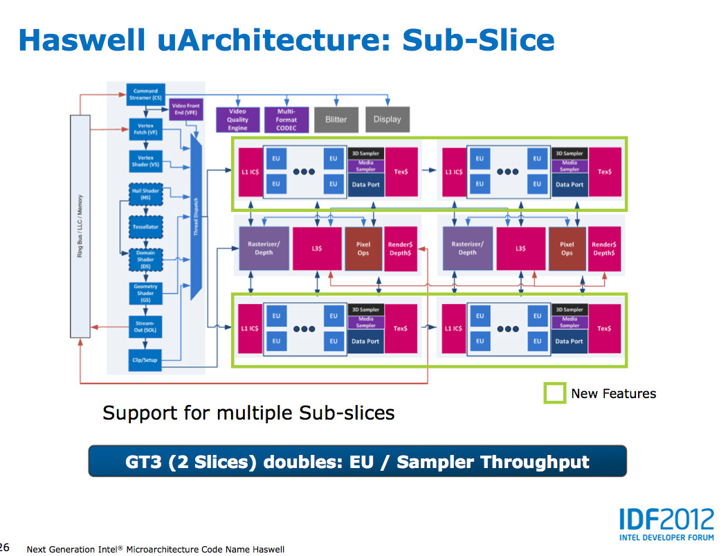
At the shader core level, Intel separates the GPU design into two sections: slice common and sub-slice. Slice common includes the rasterizer, pixel back end and GPU L3 cache. The sub-slice includes all of the EUs, instruction caches and EUs.
In Haswell GT1 and GT2 there's a single slice common, while GT3 sees a doubling of slice common. GT3 similarly has two sub-slices, although once again Intel isn't talking specifics about EU counts or clock speeds between GT1/2/3.
The final bit of detail Intel gave out about Haswell's GPU is the texture sampler sees up to a 4x improvement in throughput over Ivy Bridge in some modes.
Now to the things that Intel didn't let loose at IDF. Although originally an option for Ivy Bridge (but higher ups at Intel killed plans for it) was a GT3 part with some form of embedded DRAM. Rumor has it that Apple was the only customer who really demanded it at the time, and Intel wasn't willing to build a SKU just for Apple.
Haswell will do what Ivy Bridge didn't. You'll see a version of Haswell with up to 128MB of embedded DRAM, with a lot of bandwidth available between it and the core. Both the CPU and GPU will be able to access this embedded DRAM, although there are obvious implications for graphics.
Overall performance gains should be about 2x for GT3 (presumably with eDRAM) over HD 4000 in a high TDP part. In Ultrabooks those gains will be limited to around 30% max given the strict power limits.
As for why Intel isn't talking about embedded DRAM on Haswell, your guess is as good as mine. The likely release timeframe for Haswell is close to June 2013, there's still tons of time between now and then. It looks like Intel still has a desire to remain quiet on some fronts.


245 Comments
View All Comments
random2 - Saturday, October 6, 2012 - link
"The race to the bottom that we've seen in the LCD space made it unlikely that any of the panel vendors would be jumping at the opportunity to make their products more expensive."It's unfortunate, because of what might have been had the manufacturers, of which there are only three main ones, if I recall, had the foresight to market to customers that weren't just looking to buy the lowest priced panel on display at Best Buy. Had they the initiative to have started years ago, there would be some pretty fantastic panels available today for much more reasonable prices than seen for the 27 and 30 inch 2560X1600 panels today.
Klugfan - Saturday, October 6, 2012 - link
This doesn't really belong in the Haswell article, but I would love to know more about the physics and constraints of TDP. Like, hit me with a chart of TDP impact for a variety of important parts in phones, tablets, laptops, and desktops. Show me a chart of TDP budgets and mitigation strategies. Explain to me roughly how physics forces those things to relate. Please.Seems important and it's easy to understand the comparison from Ivy Bridge to Haswell but that doesn't feel like the big picture.
havoti97 - Saturday, October 6, 2012 - link
I read the 1st page then got bored. Writing style is overly wordy... am I the only the feeling this way?xeizo - Saturday, October 6, 2012 - link
It's an article, not a twitter feed! Some of us like to get the whole picture not just the flashy stuff ....watersb - Saturday, October 6, 2012 - link
Phenomenal feature, Anand! This is why I check your site each day. Thanks very much!bill4 - Saturday, October 6, 2012 - link
like atom, you're stuck in no mans land. way too high for tablets and phones, but in desktops and laptop, who cares if the amd solution uses 30 watts instead of 8? that difference isn't enough to matter when you take the whole platform into account, especially at lower price points where battery life wont be fantastic anyway. on the dsktop it's completely pointless.JlHADJOE - Sunday, October 7, 2012 - link
On a laptop using 30 watts instead of 8 will more than triple your battery life, especially at lower price points/smaller form factors where manufacturers gimp the battery.How's about browsing for 9 hours instead of 3? Or 27 hours instead of 9? I'd jump on it in a heartbeat.
1008anan - Saturday, October 6, 2012 - link
Haswell will sport 32 single precision or 16 double precision flops per cycle per core for its desktop and high tdp mobile skews [at least 30 watt and up].Can anyone speculate on how many single precision and double precision flops per cycle per core Haswell will execute for its low TDP skews? For example the less than 10 watt skews? the 15 watt skews?
I would also be interested in learning speculation about how many execution units (or shader cores if you prefer standard nomenclature) the low TDP Haswell products will have.
1008anan - Saturday, October 6, 2012 - link
Haswell will be able to execute 16 double precision or 32 single precision flops per clock per core for desktop and high TDP mobile skews [at least 30 watts and up].Can anyone speculate on how many flops per cycle per core the sub 10 watt and 15 watt Haswell skews will execute? Similarly I would be interested in hearing speculation about how many graphic execution units (shader cores) the sub 10 watt and 15 watt Haswell products will come with. Any speculation on graphics clock speed?
Is it possible that the high end tock 22 nm Xeon server parts could have 32 double precision or 64 single precision flops per clock per core?
Laststop311 - Saturday, October 6, 2012 - link
Best explanation of haswell I've read to date. Good Job Anand.