Intel's Haswell Architecture Analyzed: Building a New PC and a New Intel
by Anand Lal Shimpi on October 5, 2012 2:45 AM ESTHaswell's Wide Execution Engine
Conroe introduced the six execution ports that we've seen used all the way up to Ivy Bridge. Sandy Bridge saw significant changes to the execution engine to enable 256-bit AVX operations but without increasing the back end width. Haswell does a lot here.
Just as before, I put together a few diagrams that highlight the major differences throughout the past three generations for the execution engine.
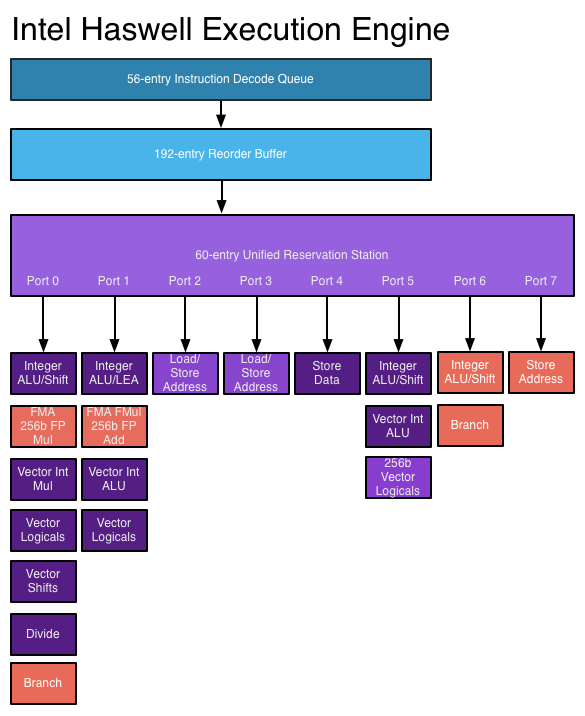
The reorder buffer is one giant tracking structure for all of the micro-ops that are in various stages of execution. The size of this buffer is directly impacted by the accuracy of the branch predictor as that will determine how many instructions can be kept in flight at a given time.
The reservation station holds micro-ops as they wait for the data they need to begin execution. Both of these structures grow by low double-digit percentages in Haswell.
Simply being able to pick from more instructions to execute in parallel is one thing, we haven't seen an increase in the number of parallel execution ports since Conroe. Haswell changes that.
From Conroe to Ivy Bridge, Intel's Core micro-architecture has supported the execution of up to six micro-ops in parallel. While there are more than six execution units in the system, there are only six ports to stacks of execution units. Three ports are used for memory operations (loads/stores) while three are on math duty. Over the years Intel has added additional types and widths of execution units (e.g. Sandy Bridge added 256-bit AVX operations) but it hasn't strayed from the 6 port architecture.
Haswell finally adds two more execution ports, one for integer math and branches (port 6) and one for store address calculation (port 7). Including both additional compute and memory hardware is a balanced decision on Intel's part.
The extra ALU and port does one of two things: either improve performance for integer heavy code, or allow integer work to continue while FP math occupies ports 0 and 1. Remember that Haswell, like its predecessors, is an SMT design meaning each core will see instructions from up to two threads at the same time. Although a single app is unlikely to mix heavy vector FP and integer code, it's quite possible that two applications running at the same time may produce such varied instructions. Having more integer ALUs is never a bad thing.
Also using port 6 is another unit that can handle x86 branch instructions. Branch heavy code can now enjoy two independent branch units, or if port 0 is occupied with other math the machine can still execute branches on port 6. Haswell moved the original Core branch unit from port 5 over to port 0, the most capable port in the system, so a branch unit on a lightly populated port makes helps ensure there's no performance regression as a result of the change.
Sandy Bridge made ports 2 & 3 equal class citizens, with both capable of being used for load or store address calculation. In the past you could only do loads on port 2 and store addresses on port 3. Sandy Bridge's flexibility did a lot for load heavy code, which is quite common. Haswell's dedicated store address port should help in mixed workloads with lots of loads and stores.
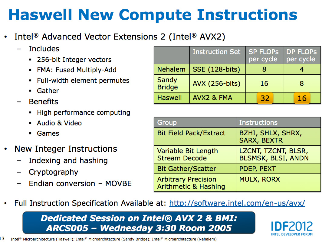
The other major addition to the execution engine is support for Intel's AVX2 instructions, including FMA (Fused Multiply-Add). Ports 0 & 1 now include newly designed 256-bit FMA units. As each FMA operation is effectively two floating point operations, these two units double the peak floating point throughput of Haswell compared to Sandy/Ivy Bridge. A side effect of the FMA units is that you now get two ports worth of FP multiply units, which can be a big boon to legacy FP code.
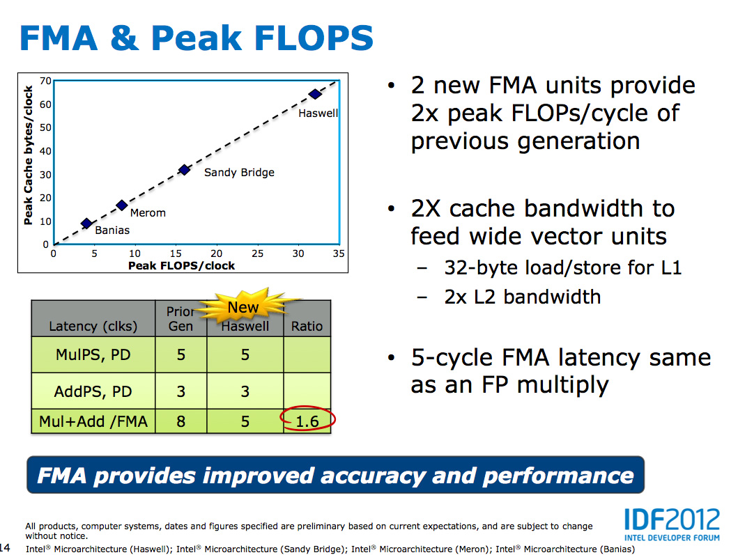
Fused Multiply-Add operations are incredibly handy in all sorts of media processing and 3D work. Rather than having to independently multiply and add values, being able to execute both in tandem via a single execution port increases the effective execution width of the machine. Note that a single FMA operation takes 5 cycles in Haswell, which is the same latency as a FP multiply from Sandy/Ivy Bridge. In the previous generation a floating point multiply+add took 8 cycles, so there's a good latency improvement here as well as the throughput boost from having two FMA units.
Intel focused a lot on adding more execution horsepower in Haswell without creating a power burden for legacy use cases. All of the new units can be shut off when not in use. Furthermore, Intel went in and ensured that this applied to the older execution units as well: in Haswell if you're not doing work, you're not consuming power.


245 Comments
View All Comments
kukreknecmi - Friday, October 5, 2012 - link
I hope i know it right. L3 on SB/IB doest used by GPU. L3 still servers as cache on system via memory controller. If GPU nneds to acess to memory, it sends request to memory controller. L3 is not directly accessable to GPU as a texture cache etc.On IB, they added a 512k cache which is seperated to half, 256k of it is used as texture system as backfeeding and other 256k half is used for other things.Article implies that L3 cache on IB is used as a texture buffer like on ordinary graphic cards. Only on Haswell L3 cache will be accessable and can be used as a some kind of GPU specific buffer.
Kevin G - Friday, October 5, 2012 - link
The confusing thing is that consumer Ivy Bridge parts have a L3 cache just for the GPU which is separate memory than the L3 cache that the CPU uses. The Ivy Bridge GPU's can use the CPU's L3 cache as the GPU's L4 cache to a degree.To confuse things further, the CPU side really has four levels of cache too. There is the small 1.5 KB micro-uop cache for instructions which comes before the 32 KB L1 instruction cache.
mayankleoboy1 - Friday, October 5, 2012 - link
From the article, its not very clear : Which platform (DT, Mobile, ultra mobile) will have the integrated voltage regulators/controllers ?Ryan Smith - Friday, October 5, 2012 - link
Ultra Mobile.Anand Lal Shimpi - Friday, October 5, 2012 - link
It's not clear how much of the VR circuitry gets integrated into Haswell or necessarily which parts will have it and which ones won't. Ultra mobile is a shoe in, but I've even heard of desktop parts getting it as well. We'll have to wait and see.DanNeely - Friday, October 5, 2012 - link
Rats. Reading the article I was hoping that Intel had decided to only bake the VRMs into their ultra-mobile parts. Better VRMs are an important factor in high end OCing; with desktop boards not cramped for space I really hope Intel keeps them off the package.Peanutsrevenge - Friday, October 5, 2012 - link
Seconded.However, I wonder whether the VRMs on high end mobos will still be an option, where the on package VRMs will simply extend the capabilities?
But given Intels recent distaste for overclocking, it wouldn't suprise me if we'll soon see CPUs completely locked from overclocking completely or only on E series, high profit chips.
Homeles - Saturday, October 6, 2012 - link
"However, I wonder whether the VRMs on high end mobos will still be an option, where the on package VRMs will simply extend the capabilities?"Bingo.
Homeles - Saturday, October 6, 2012 - link
Low end motherboards won't need them. High end overclocking boards will have them in addition to the ones on package.tuxRoller - Friday, October 5, 2012 - link
Using lvds reclocking you can reduce idle screen induced wakeups to 30 (ditto for the memory controller if the cpu supports self refresh for the sram ).eDP may allow even less.