Samsung SSD 840 (250GB) Review
by Kristian Vättö on October 8, 2012 12:14 PM EST- Posted in
- Storage
- SSDs
- Samsung
- TLC
- Samsung SSD 840
A TLC Refresher
Back in February, we published an article called Understanding TLC NAND, where we went in-depth about how NAND works and the differences between various kinds of NAND (SLC, MLC, and TLC). Back then we didn't know when TLC SSDs would be publicly available or who would be the first manufacturer. Supposedly, OCZ had interest in releasing TLC based SSDs but the supply of TLC NAND wasn't good enough for their needs. Samsung has the benefit of being a tier one manufacturer that makes its own NAND, which gives it an advantage when dealing with new technologies as it can control the output of NAND. In this case, Samsung was able to ramp up the production of TLC NAND when it wanted to, whereas OCZ must live with whatever the NAND manufacturers are ready to sell them.
While we have covered TLC in detail already, we have some new details to add:
| SLC | MLC | TLC | |
| Bits per Cell | 1 | 2 | 3 |
| P/E Cycles | 100,000 | 3,000 | 1,000 |
| Read Time | 25us | 50us | ~75us |
| Program Time | 200-300us | 600-900us | ~900-1350us |
| Erase Time | 1.5-2ms | 3ms | ~4.5ms |
Samsung would not tell us the exact read, program, and erase latencies but they told us that their TLC is around 50% slower than their MLC NAND. We don't know the latencies for Samsung's MLC NAND either, hence we have to go by general MLC NAND latencies, which varies a lot depending on process. However, we were able to get the P/E cycle count for TLC, which is 1,000. Samsung did not specify the process node but given that they listed MLC at 3,000 cycles, we are most likely talking about 27nm or 21nm. I wouldn't find it unlikely that Samsung is rating their 21nm MLC NAND at 3,000 P/E cycles as well because IMFT was able to keep the endurance at the same level with their 20nm MLC NAND.
Physically, TLC is similar to SLC and MLC. All three consist of similar transistors, the only difference is that they store a different amount of bits per cell. SLC only stores one, whereas MLC stores two and TLC stores three. This actually creates a minor problem, as there is no multiple of three that is a power of two. Unlike with hard drives, SSD capacities typically go in powers of two, such as 64GB, 128GB, and 256GB.
NAND is actually built based on binary prefixes (Mebi, Gibi...) but is almost always referred to using metric prefixes (Mega, Giga...). For example a 128GB SSD has ~137.4GB of storage (128GiB) due to Gibi to Giga translation, but the remaining space is used as spare area.
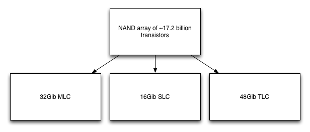
If the raw NAND array has 17.2 billion transistors, you would get 16Gibibits (17.2Gbits) of storage with SLC NAND because each cell can store one bit of data. MLC yields 32Gib, which is still a nice power of two because all you're doing is adding one level. However, with TLC you get 48Gib, which is not a power of two. Technically nothing is stopping manufacturers from making a 48Gib die, but from the marketing and engineering standpoint it's much easier to stick with powers of two. A TLC die in this case should be 32Gib just like MLC. To achieve that, the die is simply reduced in size to around 11.5 billion transistors. 32Gib isn't exactly divisible by three, but thanks to spare bits it doesn't have to be. The trick here is that the same capacity TLC die is smaller than an MLC die, which results in more dies per wafer and hence lower production costs.


86 Comments
View All Comments
JarredWalton - Monday, October 8, 2012 - link
What price are you looking at? The table shows $199.99 for the 250GB Samsung 840 (MSRP) and $249.99 for the 256GB Samsung 840 Pro.Kevin G - Monday, October 8, 2012 - link
On the fourth page:"With perfect wear-leveling and write amplification of 1x, you would get 256TiB of writes out of a 250GB Samsung 840 with TLC NAND and 1,000 P/E cycles. "
Shouldn't it be 256 GiB?
JarredWalton - Monday, October 8, 2012 - link
No; he's accounting for the visible storage capacity (and spare area). So 250GB is 256GiB of NAND but only 250GB end-user storage. You can still write 256TiB of data (256GiB * 1000 P/E), which means on a 250GB SSD you end up with the ability to write 281TB of data (for an effective P/E cycles of 1125).schizoide - Monday, October 8, 2012 - link
I'm not comfortable with TLC, particularly since it doesn't come at a huge absolute cost savings. I've been burned too often with SSDs, and now only buy the most bulletproof devices available. Maybe next generation. Maybe.Death666Angel - Tuesday, October 9, 2012 - link
I wouldn't draw any conclusion for pricing just yet. Everyone is comparing street prices of current gen SSDs to MSRP of next gen SSDs. Give it a few months to get the 840 into stores and selling and then we'll se how prices fair.I'm personally fairly confident that there will be a distinct cost advantage.
name99 - Tuesday, October 9, 2012 - link
Have ANY SSDs given you a failure based on the flash cells themselves, rather than on crappy firmware?It's stupid to demonize a technology because some companies sold you a bad product --- especially when your response is to refuse to buy a product from a company that is known (in this respect at least) NOT to have shipped crappy firmware.
harijan - Monday, October 8, 2012 - link
Pretty sure 3650GiB != 3.65TiB.3650GB == 3.65TB.
It doesn't do anything to your percentages, but this is Anandtech, we hold you to higher standards ;)
Kristian Vättö - Tuesday, October 9, 2012 - link
You are correct, I forgot that binary units don't scale up linearly (1000GiB is not 1TiB); metrics are just so much simpler. Thanks for the heads up, I've fixed the math now.iaco - Monday, October 8, 2012 - link
I wonder if Samsung will ever make a SSD made of SLC NAND. The performance would be amazing.Conficio - Monday, October 8, 2012 - link
First thanks to the Kristan and the Anand Team for another comprehensive review and the inclusion of in depth knowledge about the technology behind it.I'd like to see included in the test (or in another article) a review of the available tools for each SSD. I think it is important to know if the manufacturer supports its tools to low level format, secure erase, TRIM, ROM update etc. beyond the obligatory Windows (7). Are those available for Linux (command line and/or GUI)? Are they available for Mac OSX? Do they work if the drive is connected over USB? Are these tools user friendly to use?
It is useless if I buy an SSD and have to find out that Mac OSX does not support the tools. I have a couple of Vertex drives which I can't find a way to secure erase in order to restore full performance. They are pre TRIM drives and Mac OS X does not support trim on them anyway.
As with motherboards, the the BIOS or UEFI is important, so is with SSDs the ability to actually perform some of the low level functions. I hope you can add that to your workload! A comparison of the different tools for each manufacturer for current drives would be a great start. Thanks again!