GTC 2012 Part 1: NVIDIA Announces GK104 Based Tesla K10, GK110 Based Tesla K20
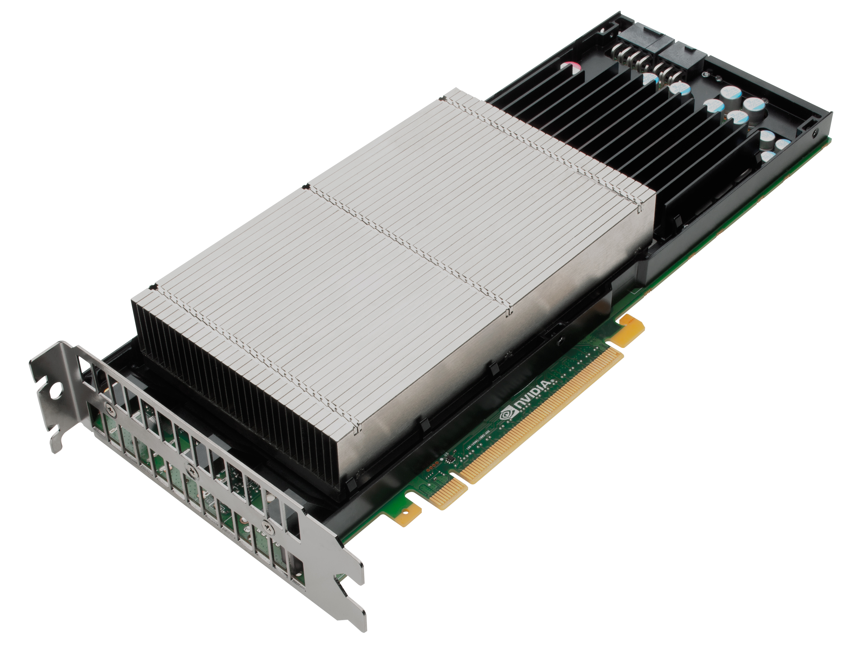
by Ryan Smith on May 17, 2012 3:15 AM ESTThe other Tesla announced this week is Tesla K20, which is the first and so far only product announced that will be using GK110. Tesla K20 is not expected to ship until October-November of this year due to the fact that GK110 is still a work in progress, but since NVIDIA is once again briefing developers of the new capabilities of their leading compute GPU well ahead of time there’s little reason not to announce the card, particularly since they haven’t attached any solid specifications to it beyond the fact that it will be composed of a single GK110 GPU.
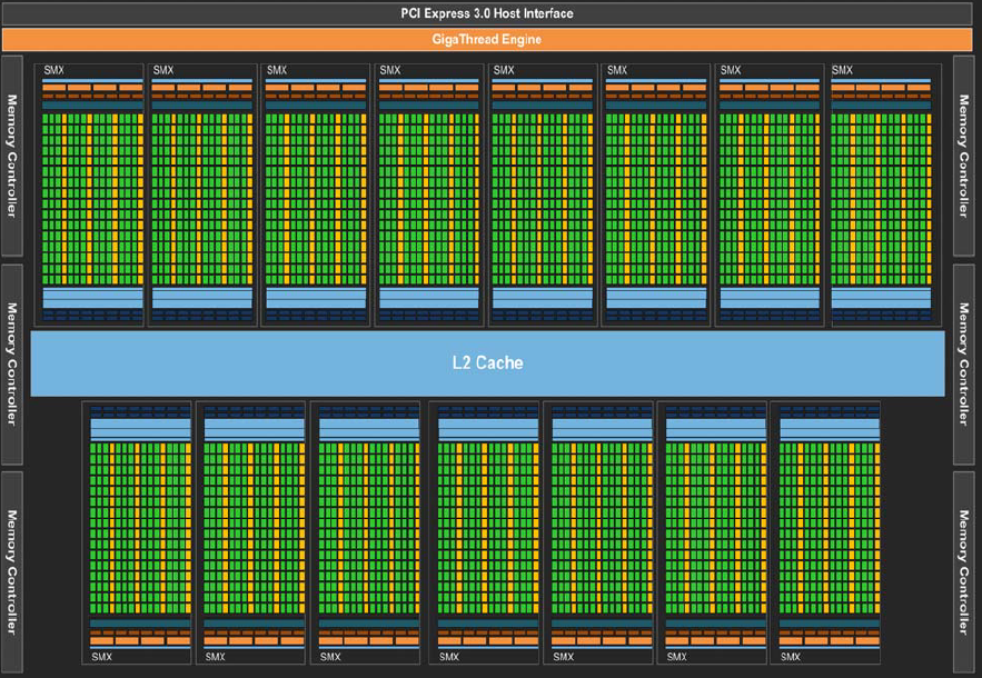
GK110 itself is a bit of a complex beast that we’ll get into more detail about later this week, but for now we’ll quickly touch upon some of the features that make GK110 the true successor to GF110. First and foremost of course, GK110 has all the missing features that GK104 lacked – ECC cache protection, high double precision performance, a wide memory bus, and of course a whole lot of CUDA Cores. Because GK110 is still in the lab NVIDIA doesn’t know what will be viable to ship later this year, but as it stands they’re expecting triple the double precision performance of Tesla M2090, with this varying some based on viable clockspeeds and how many functional units they can ship enabled. Single precision performance should also be very good, but depending on the application there’s a decent chance that K10 could beat K20, at least in the type of applications that are well suited for GK104’s limitations.
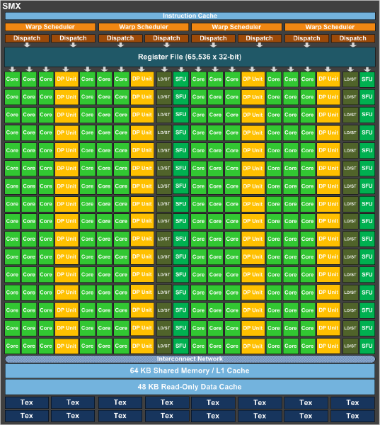
As it stands a complete GK110 is composed of 15 SMXes – note that these are similar but not identical to GK104 SMXes – bound to 1.5MB of L2 cache and a 384bit memory bus. GK110 SMXes will contain 192 CUDA cores (just like GK104), but deviating from GK104 they will contain 64 CUDA FP64 cores (up from 8, which combined with the much larger SMX count is what will make K20 so much more powerful at double precision math than K10. Of interesting note, NVIDIA is keeping the superscalar dispatch method that we first saw in GF104 and carried over to GK104, so unlike Fermi Tesla products, compute performance on K20 is going to be a little more erratic as a result of the fact that maximizing SMX utilization will require a high degree of both TLP and ILP.
Along with the slew of new features native to the Kepler family and some new Kepler family compute instructions being unlocked with CUDA 5, GK110/K20 will be bringing with it two major new features that are unique to just GK110: Hyper-Q and Dynamic Parallelism. We’ll go over both of these in depth in the near future with our look at GK110, but for the time being we’ll quickly touch on what each of them does.
Hyper-Q is NVIDIA’s name for the expansion of the number of work queues in the GPU. With Fermi NVIDIA’s hardware only supported 1 hardware work queue, whereas GK110 will support 32 work queues. The important fact to take away from this is that 1 work queue meant that Fermi could be under occupied at times (that is, hardware units were left without work to do) if there wasn’t enough work in that queue to fill every SM, even with parallel kernels in play. By having 32 work queues to select from, GK110 can in many circumstances achieve higher utilization by being able to put different program streams on what would otherwise be an idle SMX.


The other major new feature here was Dynamic Parallelism, which is NVIDIA’s name for the ability for kernels to be able to dispatch other kernels. With Fermi only the CPU could dispatch a new kernel, which incurs a certain amount of overhead by having to communicate back and forth with the CPU. By giving kernels the ability to dispatch their own child kernels, GK110 can both save time by not having to go back to the GPU, and in the process free up the CPU to work on other tasks.
Wrapping things up, there are a few other features new to GK110 such as a new grid management unit, RDMA, and a new ISA encoding scheme, all of which are intended to further improve NVIDIA’s compute performance, both over Fermi and even GK104. But we’ll save these for another day when we look at GK110 in depth.


51 Comments
View All Comments
abhishek6893 - Thursday, May 17, 2012 - link
@Ryan SmithHello. Where is this NVIDIA GTC taking place? Can't NVIDIA conduct GTC in India?
Please keep me more updated about NVIDIA's GTC. I am interested in these lectures.
Thans in advance.
Abhishek Patil,
India
Ryan Smith - Thursday, May 17, 2012 - link
GTC (prime) takes place in San Jose, California, which is NVIDIA's home city. They do hold smaller international GTC events that are focused on training, but AFAIK those have only been held in Japan and China so far.PEJUman - Thursday, May 17, 2012 - link
it's a bit unusual to see 15 SMXes instead of the usual 2^x units (16?).Seems to me they are harvesting the GK100 chips as in GTX 480 days. i.e. the chip is too big (with respect to the 28nm process capability), to be able to have enough yield for a complete 16SMXes?
It's very funny to see a company as smart as them to fall under the same pitfall twice (GTX 480 & now)
Made me wonder if Nvidia actually made a design decision on using this approach? i.e. they were planning to disable 1 or 2 SMXes right from the start, at which point, why didn't they come up with 17 SMXes design.
I assumed there is interest in the 2^x SMX units since they fit nicely on bus/buffer widths (32, 64, 128, etc).
Kevin G - Thursday, May 17, 2012 - link
The die shot that is floating around appears that it only has 15 SMX clusters instead of 16.chizow - Thursday, May 17, 2012 - link
The early leaks of the GeForce GK110 part specified 2304 SPs, which indicates only 12/15 SMX active. It could be that Nvidia is already factoring in the harvesting and TDP targets in their realized yields for GK110 wafers.We may never see a full 2880 SP Kepler, and it may have been Nvidia's intention when designing an odd numbered 15 SMX chip.
Truth of the matter is, with so many SPs, losing a few SMX would easily be the lesser of the evils if it came down to cutting functional units (see GTX 670 and GTX 680).
RussianSensation - Thursday, May 17, 2012 - link
Even with 2304 SPs and 384-bit memory bandwidth, GTX780 will be very fast.Right now GTX680 is faster than HD7970:
1536 SP vs. 2048 SP
192 GB/sec vs. 264 GB/sec bandwidth
32 ROP vs. 32 ROP
128 TMUs vs. 128 TMUs
Based on that Kepler needs 25% less SPs and 27% less memory bandwidth to compete. Even if HD8000 has 2560 SPs, 2304 SP GTX780 will still be plenty fast.
Of course if it has full blown 2,880 SPs, it will be insanely fast.
clbench - Friday, May 18, 2012 - link
HD 7970 seems faster than GTX 680 in most compute benchmarks:http://clbenchmark.com/result.jsp
CeriseCogburn - Saturday, May 19, 2012 - link
Too bad amd has little to none at all compute software to put their card to use in compute, while the will still win again in sales nVidia has a huge and supported base of the same.You gotta love that paper amd phantom compute.
Ryan Smith - Thursday, May 17, 2012 - link
K20 may ship with disabled functional units - this is part of what NVIDIA needs to figure out as they finish bringing up the chip - but GK110 as presented is complete. There are no hidden units (okay, the Polymorphs aren't on the diagram because of the audience), every functional unit is accounted for. So it's a design decision, specifically one that has an equal number of SMXs (5) for each pair of memory controllers.thebluephoenix - Thursday, May 17, 2012 - link
Can those FP64 shaders do FP32? Or when GK110 GeForce comes out they'll do just nothing in games?Also, isn't better way of building compute efficient GPU to make all shaders FP64 capable 1/1 or 1/2 FP32? Like Fermi or GCN.