The Intel SSD 710 (200GB) Review
by Anand Lal Shimpi on September 30, 2011 8:53 PM EST- Posted in
- Storage
- SSDs
- Intel
- Intel SSD 710
NAND Recap
Flash memory is non-volatile storage and in that sense it's similar to a hard drive. Once you write to a NAND flash cell it can store that data for an extended period of time without power.
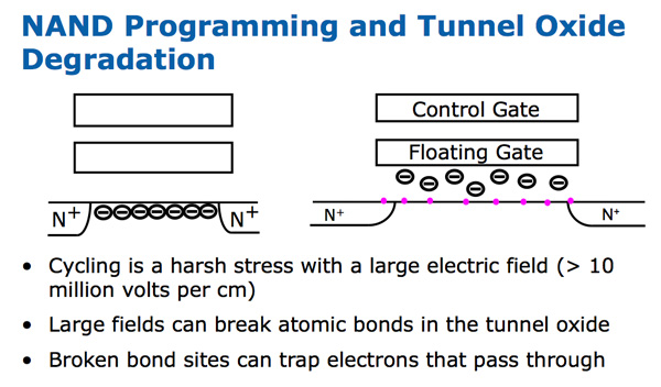
You write to NAND through a quantum tunneling process. Apply a high enough voltage across a floating-gate transistor and some electrons will actually tunnel through an insulating oxide layer and remain on the floating gate, even when the voltage is removed. Repeated tunneling can weaken the bonds of the oxide, eventually allowing electrons to freely leave the floating gate. It's this weakening that's responsible for a lot of NAND endurance issues, although there are other elements at play.
NAND is programmed and read by seeing how each cell responds to various voltages. This chart shows the difference between MLC (multi-level-cell) and SLC (single-level-cell) NAND:
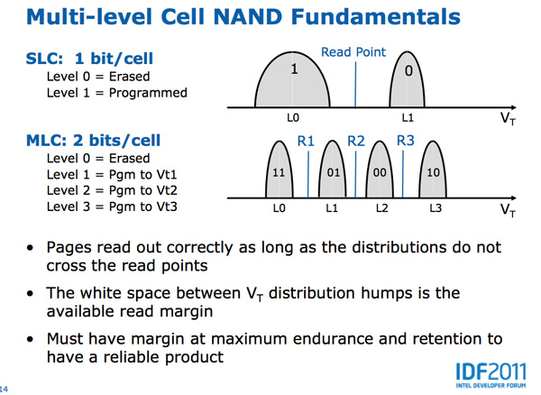
Both types of NAND are identical architecturally, it's just a question of how many voltages you map to bits on the cell. MLC (2-bit-per-cell ) has four different voltage levels that correspond to values while SLC only has two. Note that each value can correspond to a distribution of voltages. As long as the threshold voltage falls within that range, the corresponding value is programmed or read.
The white space in between each voltage distribution is the margin you have to work with. Those blue lines above are read points. As long as the voltage distributions don't cross the read points, data is accessed correctly. The bigger the margin between these points, the more write cycles you'll get out of your NAND. The smaller the margin, the easier it is to produce the NAND. It's easier to manufacture NAND that doesn't require such precise voltages to store and read data from each cell. Over time physical effects can cause these voltage distributions to shift, which ultimately leads to cell failure.
As MLC NAND gets close to the end of its life, these margins start narrowing considerably. Continuously programming and erasing NAND cells weakens the oxide, eventually allowing electrons to become stuck in the oxide itself. This phenomenon alters the threshold voltage of the transistor, which in turn shifts bit placements:
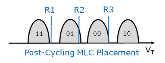
There's now ambiguity between bits which, if this cell were allowed to remain active in an SSD, would mean that when you go to read a file on your drive there's a chance that you won't actually get the data you're requesting. A good SSD should mark these bits bad at this point.
There's a JEDEC spec that defines what should happen to the NAND once its cells get to this point. For consumer applications, the NAND should remain in a read-only state that can guarantee data availability for 12 months at 30C with the drive powered off. Manufacturers must take this into account when they test and qualify their NAND. If you're curious, JEDEC also offers guidelines on how to cycle test the NAND to verify that it's compliant.
By now we all know the numbers. At 50nm Intel's MLC NAND was rated for 10,000 program/erase cycles per cell. That number dropped to 5,000 at 34nm and remained at the same level with the move to 25nm. Across the industry 3,000 - 5,000 p/e cycles for 2x-nm 2-bit-per-cell MLC (2bpc) NAND is pretty common.
For desktop workloads, even the lower end of that range is totally fine. The SSD in your desktop or notebook is more likely to die because of some silly firmware bug or manufacturing issue than you wearing out the NAND. For servers with tons of random writes, even 5K p/e cycles isn't enough. To meet the needs of these applications, Intel outfitted the 710 with MLC-HET (High Endurance Technology) more commonly known as eMLC.
Fundamentally, Intel's MLC-HET is just binned MLC NAND. SLC NAND gets away with having ultra high p/e cycle counts by only having two bit levels to worry about. The voltage distributions for those two levels can be very far apart and remain well defined over time as a result. I suspect only the highest quality NAND was used as SLC to begin with, also contributing to its excellent endurance.
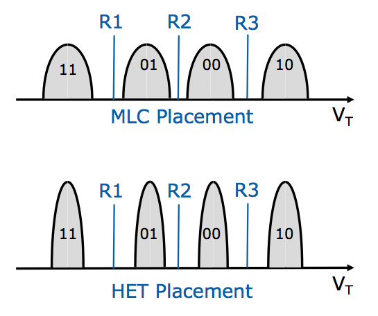
Intel takes a similar approach with MLC-HET. Placements are much more strict in MLC-HET. Remember what I said earlier, narrow ranges of voltages mapping to each bit level reduces the number of NAND die that will qualify, but you build in more margin as you cycle the NAND. If placements do shift however, Intel's SSD 710 can actually shift read points as long as the placements aren't overlapping.
Similar to frequency binning CPUs, the highest quality NAND with the tightest margins gets binned into MLC-HET while everything else is shipped as standard MLC. And just like with frequency binning, there's a good chance you'll get standard MLC that will last a lot longer than it's supposed to. In fact, I've often heard from manufacturers that hitting up to 30K p/e cycles on standard MLC NAND isn't unrealistic. With its MLC-HET Intel also more frequently/thoroughly refreshes idle NAND cells to ensure data integrity over periods of extended use.
Intel performs one other optimization on MLC-HET. After you've exceeded all available p/e cycles on standard MLC, JEDEC requires that the NAND retain your data in a power-off state for a minimum of 12 months. For MLC-HET, the minimum is reduced to 3 months. In the consumer space you need that time to presumably transfer your data over. In the enterprise world, a dying drive is useless and the data is likely mirrored elsewhere. Apparently this tradeoff also helps Intel guarantee more cycles during the drive's useful life.
At IDF Intel told us the MLC-HET in the SSD 710 would be good for around 30x the write cycles of standard (presumably 25nm) MLC. If we use 3,000 as a base for MLC, that works out to be 90K p/e cycles for Intel's 25nm MLC-HET.


68 Comments
View All Comments
cdillon - Friday, September 30, 2011 - link
I must be missing some important detail behind their decision to use MLC. MLC holds exactly twice as much information per cell as SLC, which means you can get twice the storage with the same number of chips. However, they are reserving up to 60% of the MLC NAND as spare area while still achieving a LOWER write-life than the SLC-based X25-E which only needs 20% spare. Why not continue to use lower-density SLC with a smaller spare area? The total capacity would only be slightly lower while achieving at least another 500GB of write life, if not more, and would probably also bring the 4KB Random Write numbers back up to X25-E levels.cdillon - Friday, September 30, 2011 - link
Oops, I meant to say "at least another 500TB of write life" instead of 500GB.Stahn Aileron - Saturday, October 1, 2011 - link
More than likely it has to do with production yields. Anand mentions SLC and MLC are physically identical, it's just how you address them. SLC seems to be very high quality NAND while MLC is the low end. MLC-HET (or eMLC) seems to be the middle of the pack in terms of overall quality.Unless you can get SLC yields that consistently outpace MLC-HET yields by a factor of 2, it's not very economical in the long run for the same capacity.
Also, chip manufacturing is a pretty fixed cost at the wafer level from my understanding (at least once you hit mass production on a mature process). For SLC vs MLC, you can either use double the SLC chips to match MLC capacities (higher cost) or use the same number of chips and sacrifice capacity. Intel seems to be trying to get the best of both worlds (higher capacity at the same or lower costs). (All that while maximizing their production capacity and ability to meet demand as needed as a side benefit.)
Obviously I could be wrong. That's all conjecture based on what little I know of the industry as a consumer.
ckryan - Friday, September 30, 2011 - link
Anand, thanks for the awesome Intel SMART data tip.I've joined in the XtremeSystems SSD endurance test. By writing a simulated desktop workload to the drive over and over, for months on end, eventually a drive will become read only. So far, only one drive has become RO, and that was a Samsung 470 with an apparent write amplification of 5+(this was the only SSD I've ever heard of that this has happened to outside of a lab). Another drive (a 64GB Crucial M4) has gone through almost 10,000 PE cycles, and still doesn't have any reallocated sectors -- but all of the drives have performed well, and many have hundreds of TBs on them. I chose a SF 2281 with Toshiba toggle NAND, but I'm having some issues with it (like it won't stop dropping out/or BSOD if it's the system drive). Though it takes months and months of 24/7 writing, I think the process is both interesting and likely to put many users at ease concerning drive longevity. I don't think consumers should be worrying about the endurance of 25nm NAND, but I do start wondering what will happen with the advent of next generation flash. If you want to worry about NAND, worry about sync vs async or toggle, but don't sweat the conservative PE ratings -- it seems like the controller itself plays a super important role in the preservation of NAND in addition to the NAND itself and spare area. Obviously, increasing spare area is always a good idea if you have a particularly brutal workload, but it's not a terrible idea in many other settings... it's not just for RAID0 you know.
The only real SSD endurance test takes place in a user's machine (or server), and I have no doubts that any modern SSD will last anything less than the better part of a decade -- at least as far as the flash is concerned (and probably much, much longer). You'll get mad at your SF's BSoDs and throw it out the window before you ever make a dent in the flash's lifespan. The only exception is if your drive isn't aligned (and especially without trim). Under these conditions don't expect your drive to last very long as WA jumps by double digit factors.
http://www.xtremesystems.org/forums/showthread.php...
Movieman420 - Friday, September 30, 2011 - link
Yup. And you can expect the current SF bsod problem to vanish when intel fixes it's drivers and oroms. What coincidence eh?http://thessdreview.com/latest-buzz/sandforce-driv...
JarredWalton - Saturday, October 1, 2011 - link
Ha! An educated guess in this case feels more like a pipe dream. If Intel is willing to jump on the SF controller bandwagon, I will be amazed. Then again, they've got the 510 using a non-Intel controller, so anything is possible.ckryan - Saturday, October 1, 2011 - link
It kinda makes sense though. Intel using a Sandforce controller (or possibly "Sandforce-eque") but with their firmware and NAND would be tough to stop. The SF controller (when it works -- In my case not always that often) yields benefits to consumer and enterprise workloads alike. Further, it could help bridge Intel into smaller process NAND with about the same overall TBW due to compression (My 60GB has about 85TB host to ~65TB nand writes). That's not a small amount over the lifespan of a drive. Along with additional overprovisioning, Intel could conceivably make a drive with sub-25nm NAND last as long as the 34nm stuff with those two advantages.There's nothing really stopping SF now except for the not-so little stability issues. I thought it was much rarer that it actually is (it's rare when it happens to someone else and an epidemic when it happens to you). With that heinous hose-beast no longer lurking in the closet, SandForce could end up being the only contender. Until such time as they get the problems resolved, whether or not you have problems is just a crapshoot... no seeming rhyme or reason, almost -- but not quite -- completely random. If Intel could bring that missing link to SF it would be a boon to consumers, but Intel could just as well buy SandForce to get rid of them. Either is just as likely, and conspiracy theorists would say that Intel is purposely causing issues with SF drives so they don't have to buy them (or don't have to pay as much). In the end, most consumers would just be happy if the 2281 powered drives they already have worked like the drive it was always mean to be.
Movieman420 - Saturday, October 1, 2011 - link
Guess you didn't follow the story over to VR Zone either. It's a done deal. Cherryville is SandForce 2200. It should be announced before long imo.rishidev - Friday, September 30, 2011 - link
Why even bother to make a 200gb drive at this point of time.AMD fanboys get abused for masturbating .
So What ?? im supposed to buy a $1300 Intel ""WOOOW" ssd drive.
TheSSDReview - Saturday, October 1, 2011 - link
Because Intel wants to hit the enthusiast market. The new drives wont be anywhere near the price of these 710 series drives and will demand product confidence as Intel has always had such. It is a win-win for SF since many have taken comfort in speculation of controller troubles rather than examining other such causes.The question then becomes one of SF purchase we think.