NVIDIA's Tegra 2 Take Two: More Architectural Details and Design Wins
by Anand Lal Shimpi on January 5, 2011 2:51 PM EST- Posted in
- Smartphones
- Motorola Droid
- Tegra 2
- LG
- Optimus 2X
- ATRIX 4G
- Mobile
- NVIDIA
The CPU: A Dual-Core ARM Cortex A9
NVIDIA is a traditional ARM core licensee, which means it implements ARM’s own design rather than taking the instruction set and designing its own core around it (ala Qualcomm).
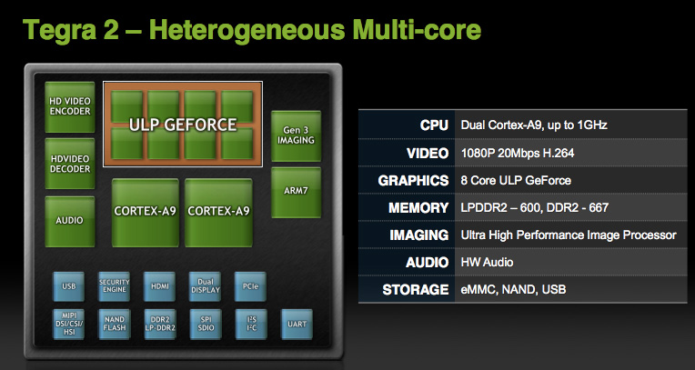
The Tegra 2 SoC has a pair of ARM Cortex A9s running at up to 1GHz. The cores are clock gated but not power gated. Clock speed is dynamic and can be adjusted at a very granular level depending on load. Both cores operate on the same power plane.
Architecturally, the Cortex A9 isn’t very different from the Cortex A8. The main change is a move from a dual-issue in order architecture with the A8 to a dual-issue out-of-order architecture with the A9.
With its OoO architecture, the A9 adds a re-order buffer and 16 more general purpose registers over the A8 for register renaming. Cortex A9 can reorder around write after read and write after write hazards.
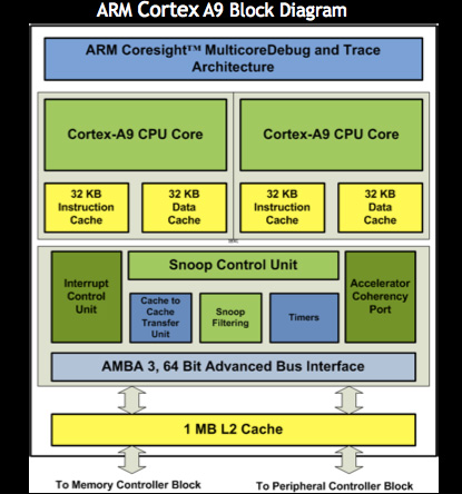
ARM’s Cortex A9 MPcore architecture supports up to four cores behind a single shared L2 cache (at up to 1MB in size). Tegra 2 implements a full 1MB shared L2 cache and two Cortex A9 cores. Each core has a 64KB L1 cache (32KB instruction + 32KB data cache).
Pipeline depth is another major change between A8 and A9. While the Cortex A8 had a 13-cycle branch mispredict penalty, A9 shortens the pipeline to 8 cycles. The shallower pipeline improves IPC and reduces power consumption. Through process technology hitting 1GHz isn’t a problem at TSMC 40nm.
From what I can tell, branch prediction, TLBs and execution paths haven’t changed between A8 and A9 although I’m still awaiting further details from ARM on this.
NVIDIA is claiming the end result is a 20% increase in IPC between A8 and A9. That’s actually a bit lower than I’d expect, but combined with the move to dual core you should see a significant increase in performance compared to current Snapdragon and A8 based devices.
If on single threaded workloads the best performance improvement we see is 20%, Qualcomm’s dual-core 1.2GHz Snapdragon due out later this year could still be performance competitive.
While all Cortex A8 designs incorporated ARM’s SIMD engine called NEON, A9 gives you the option of integrating either a SIMD engine (ARM’s Media Processing Engine, aka NEON) or a non-vector floating point unit (VFPv3-D16). NVIDIA chose not to include the A9’s MPE and instead opted for the FPU. Unlike the A8’s FPU, in the A9 the FPU is fully pipelined - so performance is much improved. The A9’s FPU however is still not as quick at math as the optional SIMD MPE.
| Minimum Instruction Latencies (Single Precision) | ||||||
| Instruction | FADD | FSUB | FMUL | FMAC | FFDIV | FSQRT |
| ARM Cortex A8 (FPU) | 9 cycles | 9 cycles | 10 cycles | 18 cycles | 20 cycles | 19 cycles |
| ARM Cortex A9 (FPU) | 4 cycles | 4 cycles | 5 cycles | 8 cycles | 15 cycles | 17 cycles |
| ARM Cortex A8 (NEON) | 1 cycle | 1 cycle | 1 cycle | 1 cycle | N/A | N/A |
| ARM Cortex A9 (MPE/NEON) | 1 cycle | 1 cycle | 1 cycle | 1 cycle | 10 cycles | 13 cycles |
NVIDIA claims implementing MPE would incur a 30% die penalty for a performance improvement that impacts only a minimal amount of code. It admits that at some point integrating a SIMD engine makes sense, just not yet. The table above shows a comparison of instruction latency on various floating point and SIMD engines in A8 and A9.
TI’s OMAP 4 on the other hand will integrate ARM’s Cortex A9 MPE. Depending on the code being run, OMAP 4 could have a significant performance advantage in some cases.


21 Comments
View All Comments
nahidalam - Wednesday, June 29, 2011 - link
Anand/Brian,Any details on the security engine tegra2 is using?