Intel's Sandy Bridge Architecture Exposed
by Anand Lal Shimpi on September 14, 2010 4:10 AM EST- Posted in
- CPUs
- Intel
- Sandy Bridge
The Front End
Sandy Bridge’s CPU architecture is evolutionary from a high level viewpoint but far more revolutionary in terms of the number of transistors that have been changed since Nehalem/Westmere.
In Core 2 Intel introduced a block of logic called the Loop Stream Detector (LSD). The LSD would detect when the CPU was executing a software loop turn off the branch predictor and fetch/decode engines and feed the execution units through micro-ops cached by the LSD. This approach saves power by shutting off the front end while the loop executes and improves performance by feeding the execution units out of the LSD.
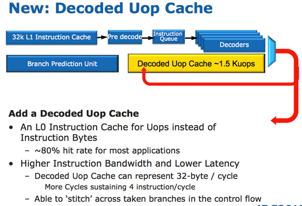
In Sandy Bridge, there’s now a micro-op cache that caches instructions as they’re decoded. There’s no sophisticated algorithm here, the cache simply grabs instructions as they’re decoded. When SB’s fetch hardware grabs a new instruction it first checks to see if the instruction is in the micro-op cache, if it is then the cache services the rest of the pipeline and the front end is powered down. The decode hardware is a very complex part of the x86 pipeline, turning it off saves a significant amount of power. While Sandy Bridge is a high end architecture, I feel that the micro-op cache would probably benefit Intel’s Atom lineup down the road as the burden of x86 decoding is definitely felt in these very low power architectures.
The cache is direct mapped and can store approximately 1.5K micro-ops, which is effectively the equivalent of a 6KB instruction cache. The micro-op cache is fully included in the L1 i-cache and enjoys approximately an 80% hit rate for most applications. You get slightly higher and more consistent bandwidth from the micro-op cache vs. the instruction cache. The actual L1 instruction and data caches haven’t changed, they’re still 32KB each (for total of 64KB L1).
All instructions that are fed out of the decoder can be cached by this engine and as I mentioned before, it’s a blind cache - all instructions are cached. Least recently used data is evicted as it runs out of space.
This may sound a lot like Pentium 4’s trace cache but with one major difference: it doesn’t cache traces. It really looks like an instruction cache that stores micro-ops instead of macro-ops (x86 instructions).
Along with the new micro-op cache, Intel also introduced a completely redesigned branch prediction unit. The new BPU is roughly the same footprint as its predecessor, but is much more accurate. The increase in accuracy is the result of three major innovations.
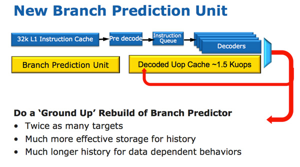
The standard branch predictor is a 2-bit predictor. Each branch is marked in a table as taken/not taken with an associated confidence (strong/weak). Intel found that nearly all of the branches predicted by this bimodal predictor have a strong confidence. In Sandy Bridge, the bimodal branch predictor uses a single confidence bit for multiple branches rather than using one confidence bit per branch. As a result, you have the same number of bits in your branch history table representing many more branches, which can lead to more accurate predictions in the future.
Branch targets also got an efficiency makeover. In previous architectures there was a single size for branch targets, however it turns out that most targets are relatively close. Rather than storing all branch targets in large structures capable of addressing far away targets, SNB now includes support for multiple branch target sizes. With smaller target sizes there’s less wasted space and now the CPU can keep track of more targets, improving prediction speed.
Finally we have the conventional method of increasing the accuracy of a branch predictor: using more history bits. Unfortunately this only works well for certain types of branches that require looking at long patterns of instructions, and not well for shorter more common branches (e.g. loops, if/else). Sandy Bridge’s BPU partitions branches into those that need a short vs. long history for accurate prediction.


62 Comments
View All Comments
JoJoman88 - Wednesday, September 15, 2010 - link
To me the problem is that instead of me overclocking without reguard to TDP, now Intel will do the overclocking for me, but it will be within the TDP that Intel thinks is best. Will this not just kill the after-market cooler makers with an almost locked TDP,and to some degree high end memory maker with a locked BCLK.This will change how overclocking is done from now on unless AMD keeps things as they are and forces Intel from going down this road.
gvaley - Wednesday, September 15, 2010 - link
It's true that the CPU will turboboost within the CPU's TDP, but exactly how much it will turboboost (how much bins it will gain) will depend on how well the CPU is being chilled. So having a better (read: aftermarket) cooler will allow you to take the best of your CPU's turboboost.shodanshok - Wednesday, September 15, 2010 - link
Hi Anand,while I expect the ring bus to provide great performances, I doubt that it don't impact die size and power consumption in respect to the Nehalem/Westmere L3 organization.
Let me explain...
From my internal test, the Nehalem/Westmere L3 cache seems accessed by a four 64 bit channels (one per core). At 3 Ghz L3 cache, it translate in a maximum of 24 GB/s per core, or 96 GB/s for 4 cores. This cache organization seems confirmed by the tests at Techreport (on a i975X, SANDRA's L3 cumulative bandwidth is at about 60 GB/s: http://www.techreport.com/articles.x/18581/5) and Xbitlabs (EVEREST single-core L3 bandwidth of about 20 GB/s: http://www.xbitlabs.com/articles/cpu/display/intel...
So, on Nehalem/Westmere I do not expect 4 x 256 wires, but only 4 x 64 wires (more or less).
Now, lets examine SB...
We have 4 x 256 bit bus (4 indipendent rings) that runs around the L3 cache, for a total of 1024 wires. So, we have a lot of wires, that needs to be powered. These wires, in turn, need additional die space, and to me seems the main reason why most models will have "only" a 6 MB L3.
What do you think about? It is possible to ask Intel something about the Nehalem L3 cache organization and/or about the decision to equip most SB models with 6 MB of L3 cache?
Thanks.
Casper42 - Wednesday, September 15, 2010 - link
Knowing what you do about Nehalem EX and SNB on socket H2, any speculation on what we can expect from the Socket B2/R chips when they finally arrive sometime next year?I am mainly thinking of Northbridge/QPI and PCIe Lanes as compared to DMI used on the Mainstream parts discussed in this article.
I waited and waited for Westmere Core i7 to become "cheap" and thought the 970 was going to be my chip of choice @ $550. When they released it at $900 (you could already find 980Xs for less) it pretty much killed my plans to upgrade.
So now I am basically debating on do I build a high end H2 or wait for the enthusiast version to arrive instead?
My understanding from seeing the server roadmap is there will be Socket B2 and Socket R with the differences between them mainly consisting of memory channels and # of PCIe Lanes. I have also read that both will support PCIe 3.0 whereas H2 will continue to use 2.0.
Add all these changes up and I am also hopeful we will see USB3 on the Enthusiast platform as well since it will have an additional 3-6 months to mature.
So any ideas/insight you have here would be awesome.
linkages - Thursday, September 16, 2010 - link
With the price of LCDs dropping, I am noticing that more and more consumers have more than one display for their mainstream machines. Has Intel said anything about how many displays the onboard graphics will be able to push? Have they said anything about what tech they are going to use ie. display port, HDMI, DVI-D, something else?I can see myself getting a new SB machine sometime in Q1 2011 but I run at least 2 monitors at all times ( need the real estate for the type of work that I do ). I don't play many games but having the video decode/encode is important to me since I do tend to do some videoconferencing now a days.
The last thing I would like to know is if Intel is going to do the right thing with the drivers for their graphics. Will we humble linux users finally have a graphics driver that does not suck. Will Intel finally open source the driver so that the community can keep it updated and optimize it for X?
chukked - Thursday, September 16, 2010 - link
Hi Anand,thanks for the review, you addressed everything but left virtualization :(
which processors support vt-x and vt-d ?
iwodo - Friday, September 17, 2010 - link
x264, the best h.264 encoder there is, produce better quality video and similar speed when using "ultrafast" setting. And with 2 / 4 Core we could even transcode 2 - 4 video at the same time.The hardware encoder inside SandyBridge is not that speedy. While i could scarifies quality for speed. But Power VR's VRE Core manage 1000fps +, @ 400fps the encoder is like a waste of die space.
Intel could have further tuned the x264 for Sandy Bridge for speed and just release it with their drivers. If the hardware encoder aren't giving many times the increase in speed, then what is the point? They may as well have added extra 6 EU for GPU inside.
A Link to someone's blog posting some figures.
http://lee.hdgreetings.com/2010/09/intel-cpu-vs-nv...
Wolfpup - Wednesday, September 29, 2010 - link
Pretty disappointing. I'm sure AMD's glad though!10-30% improvement-obviously that's great, but not as big as their previous tocks if I'm remembering right, and not much different from what "ticks" like Penryn did...I know Penryn was like a 10% boost minimum over Conroe...
I'm guessing it's because they're wasting effort and die area on a worthless GPU. I *HOPE* no one on this site, no power users are going to be using that thing. (Well, okay, for a tiny notebook or something maybe...)
JumpingJack - Wednesday, September 29, 2010 - link
I don't believe you are remembering correctly.Conroe was the first tock, and certainly, it was a major leap over the P4 line. But it's bloodline was actually derived from P6, which was carried through from Banias, Dothan, then Yohna. The improvement over Yohna was in the 10-20% IPC range.
Then came Penryn the tick, which was on average only 5%, http://www.anandtech.com/show/2306/3
Then came the tock, which was Nehalem. In single threaded performance, it was roughly another 5-10% over Penryn, but in multithreaded -- again, clock for clock, it had leaps of performance, around 20-40% again. http://www.anandtech.com/show/2658/20
The tick of Nehalem was Westmere, now Westmere did not launch a quad core part so it is hard to find a clock for clock, but in single threaded performance -- roughly the same as Nehalem, factoring out any turbo advantages...
Now SB, a tick, with another 10-30% across the board both single and multithreaded, depending on workload.
Of course, the GPU is not so worthless, it is indeed challenging low end GPUs -- no doubt Llano will offer up strong GPU performance, but for the majority of the market SB is perfectly fine.
Indeed, AMD is not too happy here, at least I would suspect. On the CPU side, Intel will crush anything AMD has in the same market segement where SB resides... GPU, surely AMD will crush SB. On the CPU front, AMD is already 20-40% behind Nehalem clock for clock, core for core, SB just extends that another 10-30%.
gundersausage - Tuesday, October 26, 2010 - link
i7-950 vs i7-2500K... So which will be faster and a better gaming chip? anyone?