Intel's Sandy Bridge Architecture Exposed
by Anand Lal Shimpi on September 14, 2010 4:10 AM EST- Posted in
- CPUs
- Intel
- Sandy Bridge
Sandy Bridge Graphics
The largest performance improvement on Sandy Bridge vs. current Westmere architectures actually has nothing to do with the CPU, it’s all graphics. While the CPU cores show a 10 - 30% improvement in performance, Sandy Bridge graphics performance is easily double what Intel delivered with Clarkdale/Arrandale at the beginning of the year.
While the ‘dales improved performance by moving graphics to a 45nm process, increasing shader hardware and clock speed, SNB graphics improves through a significant increase in IPC.
The Sandy Bridge GPU is on-die built out of the same 32nm transistors as the CPU cores. The GPU is on its own power island and clock domain. The GPU can be powered down or clocked up independently of the CPU. Graphics turbo is available on both desktop and mobile parts, and you get more bins with graphics turbo on Sandy Bridge than you did with Arrandale.
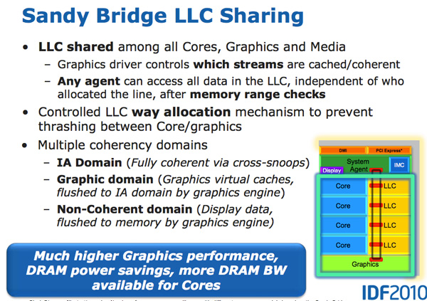
The GPU is treated like an equal citizen in the Sandy Bridge world, it gets equal access to the L3 cache. The graphics driver controls what gets into the L3 cache and you can even limit how much cache the GPU is able to use. Storing graphics data in the cache is particularly important as it saves trips to main memory which are costly from both a performance and power standpoint. Redesigning a GPU to make use of a cache isn’t a simple task. It usually requires the sort of complete re-design that NVIDIA did with GF100 for example.
SNB graphics is the anti-Larrabee. While Larrabee focused on extensive use of fully programmable hardware (with the exception of the texture hardware), SNB graphics (internally referred to as Gen 6 graphics) makes extensive use of fixed function hardware. The design mentality was anything that could be described by a fixed function should be implemented in fixed function hardware. The benefit is performance/power/die area efficiency, at the expense of flexibility. Keeping much of the GPU fixed function is in-line with Intel’s CPU centric view of the world. By contrast, taking the GPU as programmable as possible makes more sense for a GPU focused company like NVIDIA.
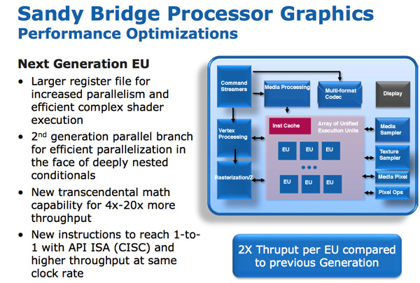
The programmable shader hardware is composed of shaders/cores/execution units that Intel calls EUs. Each EU can dual issue picking instructions from multiple threads. The internal ISA maps one-to-one with most DirectX 10 API instructions resulting in a very CISC-like architecture. Moving to one-to-one API to instruction mapping increases IPC by effectively increasing the width of the EUs.
There are other improvements within the EU. Transcendental math is handled by hardware in the EU and its performance has been sped up considerably. Intel told us that sine and cosine operations are several orders of magnitude faster now than they were in current HD Graphics.
In previous Intel graphics architectures the register file was repartitioned on the fly. If a thread needed fewer registers, the remaining registers could be allocated to another thread. While this was a great approach for saving die area, it proved to be a limiter for performance. In many cases threads couldn’t be worked on as there were no registers available for use. Prior to Intel HD Graphics each thread had an average of 64 registers, the ‘dales brought that average up to 80 per thread. In SNB, the GPU has a fixed amount of registers per thread: 120. The register count limiting thread count scenarios have been alleviated.
All of these enhancements result in 2x the instruction throughput per EU compared to Intel’s HD Graphics today.

Sandy Bridge vs. NVIDIA GeForce 310M Playing Starcraft 2
At launch there will be two versions of Sandy Bridge graphics: one with 6 EUs and one with 12 EUs. All mobile parts (at launch) will use 12 EUs, while desktop SKUs may either use 6 or 12 depending on the model. From what I’ve heard, the higher end SKUs may have 12 while the lower end models will have 6 but I haven’t seen it on a roadmap yet so I can’t confirm. With a 2x improvement in throughput per EU, you should see greater than Intel HD Graphics performance even with the 6 EU parts (thanks to higher clock speeds and the GPU sharing the L3 cache).


62 Comments
View All Comments
name99 - Tuesday, September 14, 2010 - link
This is no secret. This is exactly Intel's tick-tock strategy that has been in place for years now.The one thing you have to keep in mind is that designing these CPUs now takes of order SEVEN YEARS (!!!) from conception to ship, which means that slips and mistakes do occur. Intel (and I guess AMD) have to make their best guess as to what the market will look like in seven years and sometimes they do guess incorrectly. Of course there is scope for small changes along the way closer to the release date, but not for changes in the grand strategy.
medi01 - Tuesday, September 14, 2010 - link
Agreed, it was two things: greed and the fact that AMD is currently not in a position to be a threat.tatertot - Tuesday, September 14, 2010 - link
"The value segments won’t see Sandy Bridge until 2012."You later show a roadmap slide which indicates Sandy Bridge in the value segment in Q3 2011.
Perhaps you meant "H2 '11" instead of "2012" ?
J_Tarasovic - Thursday, September 16, 2010 - link
I think that the roadmap probably refers to OEM shipments, whereas, Anand was probably referring to when consumers would actually be able to buy devices.iwodo - Tuesday, September 14, 2010 - link
I just realize that my computer will no longer scream when i do WebCam Video Conferencing with Skype!. With the Encoder Engine and Decoder Engine, all i am doing it feeding USB 3.0 data and move them around........yuhong - Tuesday, September 14, 2010 - link
"Back in the Core Duo days that was 80-bits of data. When Intel implemented SSE, the burden grew to 128-bits. ""Core Duo" Huh?
NaN42 - Tuesday, September 14, 2010 - link
No, it seems to be right. Core Duo belongs to the Pentium M microarchitecture which implemented the SSE registers as two 64bit registers. So the largest registers were the x87-registers, but I'm not sure whether upon register renaming the registers were really copied.aka_Warlock - Tuesday, September 14, 2010 - link
New CPU from Intel... and guess what?!! New SOCKET!! Lol.Intel do know how to milk the stupid cow.
bernpi - Sunday, November 14, 2010 - link
For most people it makes perfect sense to get a new socket. Most people don't buy every new CPU from Intel or AMD because it would be a waste of money. My current CPU is a Core2Duo Quad processor with a 775 socket, i skipped the nehalem generation and will buy a SandyBridge early next year. So why should i keep my motherboard and the old 775 socket? Of course i will buy a new motherboard for the new processor. So i think for most people this is not a real issue.Sahrin - Tuesday, September 14, 2010 - link
There's a lot of "neato" stuff that does a lot to improve the user experience by making the chip use its design resources more intelligently (smarter turbo - that 'comcast turbo-boost' feature should really make a difference for end users); but in terms of actual throughput it looks like Intel left FP performance the same; and there certainly isn't any new integer hardware.K11, on the other hand, doubled integer ALU's (though the raw number of execution units is now the same as in a Nehalem core) and added a half-width (compared to Intel) FP unit.
First, I'd be interested to see if the whizz-bangies AMD was talking about for the K11 FPU a year ago make the execution time for 128-bit FP instructions comparable, better than, or still slower than Intel's FPU .
Second, I'd be quadruple interested to see what impact the way AMD is allocating the new integer hardware is going to have on performance. A monolithic Nehalem core is going to be able to handle more complex (wider) threads better than a K11 core (that's a 2-integer and 1-FPU Bulldozer); but in SMT-mode (or pseudo-SMT mode) what happens? We know Intel experiences a performance hit in HTT mode which they are only able to offset because Nehalem is so wide. AMD thinks it isn't going to get the expected hit in the front end, and they won't have the thread-switching penalty that Intel does. My prediction is that 8-core K11/Bullzoder will crush Sandy Bridge in multithreaded FP-light workloads and be 5-20% slower in everything else (the possible exception being 128-bit floats).
I'm actually kind of disappointed by this update to Nehalem...Intel did a lot of "uncore" stuff and implemenated AVX. Where's our wider back-end? More execution hardware drives better single-thread performance...the rest is just undoing the damage from the CISC-RISC transition in the front end and OoO .