NVIDIA’s GeForce GTS 450: Pushing Fermi In To The Mainstream
by Ryan Smith on September 13, 2010 12:02 AM EST- Posted in
- NVIDIA
- Fermi
- GeForce GTS 450
- GF106
- GPUs
After the drawn out launch of GF100 and the GTX 400 series earlier this year, NVIDIA has been firing on all cylinders when it comes to the launch of the rest of the Fermi family. In July we saw the launch of the GF104 GPU and the GTX 460 it powers, providing a surprising tweak to the Fermi architecture on what should have been a simple waterfall part, and in the process trampling AMD’s Radeon HD 5830 at the $200 price point. For the first time in over a year we saw an NVIDIA product come out that was hyper-competitive on performance and pricing, the kind of competition we sorely miss.
Now 2 months after that launch we’re going to find out if lightning strikes twice. Today NVIDIA is launching the next desktop video card in the 400 series: GTS 450 Powering it is their new Fermi family GPU – GF106 – the next in the line of successively smaller Fermi GPUs for cheaper products. Targeted directly against AMD’s Radeon HD 5700 series, does it have what it takes to dethrone AMD's mainstream lineup?
| GTX 480 | GTX 460 768MB | GTX 285 | GTS 450 | GTS 250 | |
| Stream Processors | 480 | 336 | 240 | 192 | 128 |
| Texture Address / Filtering | 60/60 | 56/56 | 80 / 80 | 32/32 | 64/64 |
| ROPs | 48 | 24 | 32 | 16 | 16 |
| Core Clock | 700MHz | 675MHz | 648MHz | 783MHz | 738MHz |
| Shader Clock | 1401MHz | 1350MHz | 1476MHz | 1566MHz | 1836MHz |
| Memory Clock | 924MHz (3696MHz data rate) GDDR5 | 900MHz (3.6GHz data rate) GDDR5 | 1242MHz (2484MHz data rate) GDDR3 | 902MHz (3.608GHz data rate) GDDR5 | 1100MHz (2.2GHz data rate) GDDR3 |
| Memory Bus Width | 384-bit | 192-bit | 512-bit | 128-bit | 256-bit |
| Frame Buffer | 1.5GB | 768MB | 1GB | 1GB | 1GB |
| FP64 | 1/8 FP32 | 1/12 FP32 | 1/12 FP32 | 1/12 FP32 | N/A |
| Transistor Count | 3B | 1.95B | 1.4B | 1.17B | 754M |
| Manufacturing Process | TSMC 40nm | TSMC 40nm | TSMC 55nm | TSMC 40nm | TSMC 55nm |
| Price Point | $499 | $169 | N/A | $129 | $99 |
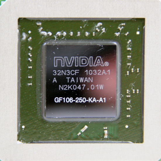
At the heart of the GTS 450 is the GF106 GPU, which is probably not one of NVIDIA’s best-kept secrets. Traditionally GPUs launch in desktop products first before getting the mobile treatment, but in the case of the 400 series it’s a bit of the inverse. GF100 and GF104 launched in desktop products first, but GF106 and GF108 were launched in a somewhat quiet manner earlier this month when NVIDIA unveiled their mobile 400 series lineup. So GF106 itself is not being unveiled today, but we do have more concrete details about it that weren’t available for the mobile launch.
If you recall GF104, it set itself up nicely to be cut-down for GF106. With 384 CUDA cores spread over 2 GPCs and 4 sets of ROPs & memory controllers, half of a GF104 and what presumably would be a GF106 was easy to see. Instead what we’re getting is a bit of a curveball, as GF106 is a bit more than half of a GF104.
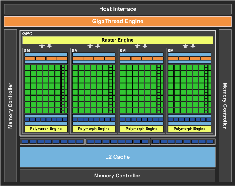
GF106 Block Diagram
Fundamentally it’s GF104-derrived, sporting the 48 CUDA cores per SM design that GF104 pioneered. But while NVIDIA did end up removing 1 of the 2 GPCs (and by extension, half the CUDA cores), they didn’t halve the ROPs and memory controllers while they were at it. As a result GF106 is a bit more than we bargained for, entering the world as a 192 CUDA core part but with 3 sets of memory controllers and ROPs, for a combined total of a 192bit memory bus, 384KB of L2 cache, and 24 ROPs. Internally this is organized as a 1 GPC part containing 4 SMs, resulting in GF106 having 1 Raster Engine and 4 Polymorph engines; meanwhile the contents of each SM remains unchanged from GF104, so for each SM there are 48 CUDA cores and 4 texture units (for a total of 16 texture units in GF106) along with its Polymorph Engine.
But like GF104, GF106 won’t immediately be seen in its full form. NVIDIA is launching their desktop GF106 cards with 1 of the 3 sets of memory controller/ROP pairs disabled. As a result GTS 450 as we know it today is going to be a 192 CUDA core part, but using a 128bit memory bus with 256KB of L2 cache and 16 ROPs. For the time being the only product that’s been announced that will use a full GF106 GPU is the GeForce GT 460M, which will be available in a 192bit configuration with all 192 CUDA cores enabled.
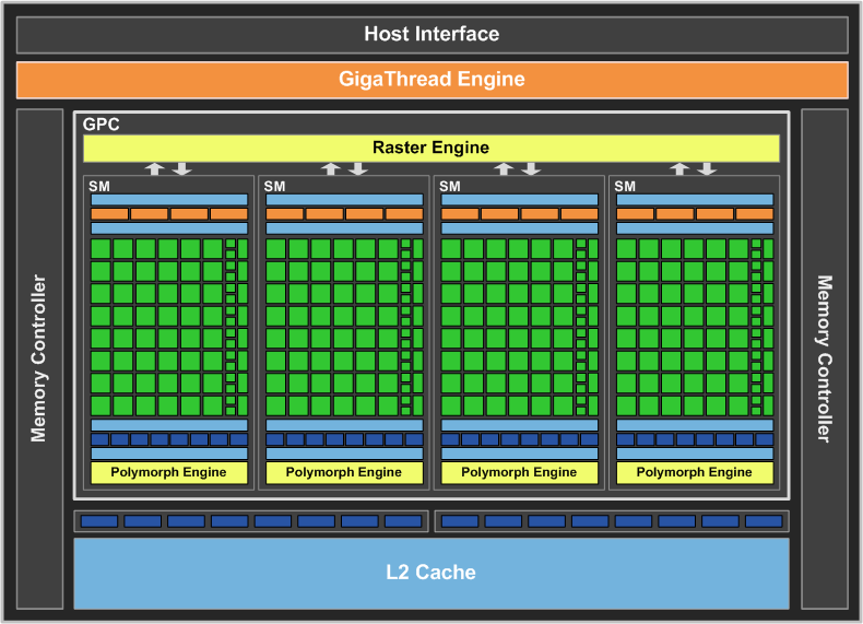
GTS 450 Block Diagram
At 1.17 billion transistors GF106 is not particularly big; NVIDIA won’t give us the die size, but a really rough estimate on our part is 240mm2(15mm x 16mm). With that in mind, we hear that 40nm yields at TSMC are caught up with 55nm yields, so we’re not entirely sure why NVIDIA is launching only harvested parts today. At first glance it seems like they could launch a 2nd, fully-equipped card for a higher price and profit margin, but admittedly we don’t have all the facts. The biggest question of course is whether enabling the extra memory controller and ROPs provides a material benefit – if GF106 is shader limited at these clockspeeds, then perhaps it isn’t worth it. Hopefully one day we’ll find out if this is the case.
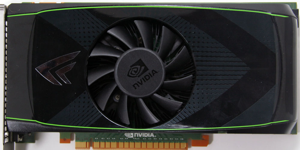
In any case, the star of the show today is GTS 450, the newest member of the GeForce family and intended for gaming at resolutions around 1680x1050. It’s clocked at 783MHz for the core, 1566MHz for the shaders, and 902MHz (3.6GHz effective) for its GDDR5 RAM. Currently it’s only being offered in a 1GB configuration; however we wouldn’t be shocked to see a 512MB part further down the line at even more budget-oriented prices. NVIDIA is launching the card at $129 and will be using it to replace the GTS 250, the last and most powerful card based on NVIDIA’s long-lived workhorse, G92. This makes GF106 the de-facto successor to G92, a very tough act to follow.
NVIDIA puts the TDP for a reference GTS 450 at 106W, though as NVIDIA likes to note this is a “real world” number and FurMark can exceed this. NVIDIA does not provide an idle TDP for GTS 450, however as you’ll see in our tests it’s clearly quite low. Like the GTX 460, NVIDIA is heavily pushing the overclockability of GTS 450, and as a result a large number of factory-overclocked cards will be launching alongside reference-clocked cards. This pushes the TDP further out but it improves performance a great deal – the fastest of the vendor cards we’re looking at today is 930MHz, a 19% factory overclock. These cards will of course command a higher price, although we hear some of the lesser overclocked cards may hit the same $129 price as the reference-clocked cards.
Finally, NVIDIA is once again repricing the 400 series lineup with this launch. The MSRP of the GTX 470 and GTX 465 are down to $300 and $230 respectively. Meanwhile GTX 460 is also getting a price drop – the 1GB version drops by $10 to $220 while the 768MB version takes a much bigger price drop of $30 to $170. At $200 the 768MB GTX 460 was already a good deal, but as we noted in our on review for $30 more it made much more sense to grab the 1GB card with its wider memory bus and additional ROPs. As a consequence NVIDIA has driven a larger price gap between the two cards so that the 768MB version isn’t passed up in favor of the 1GB version as often.
Finally we have the GTS 450, which is launching at $130. NVIDIA was clearly going for a price between the Radeon HD 5770 and 5750, however AMD apparently expected this and has worked with partners to nudge prices down – the cheapest 5770s can be found for $130 after rebate. If these prices hold then the GTS 450 is basically in lock-step with the 5770, but we’re only seeing a few 5770s at this price so it may prove to be a temporary launch day counter-attack. In any case AMD is definitely under some pricing pressure thanks to the GTX 460 price drop – the GTX 460 is significantly faster than the 5770, so they can’t realistically charge more than $150 for it and leaving them few options besides bringing prices down and putting pressure on the GTS 450.
| September 2010 Video Card MSRPs | ||
| NVIDIA | Price | AMD |
| $700 | Radeon HD 5970 | |
| $500 | ||
|
|
$360 | Radeon HD 5870 |
| $300 | ||
|
|
$270 | Radeon HD 5850 |
| $230 | ||
| $220 | ||
| $170 | Radeon HD 5830 | |
| $130 | Radeon HD 5770 | |


66 Comments
View All Comments
kallogan - Monday, September 13, 2010 - link
"Furthermore our pre-release version of Badaboom with Fermi support doesn’t work either, so that also was dropped"I knew you had a special version of badaboom for your GTX 400s reviews ;)
tviceman - Monday, September 13, 2010 - link
Great job on the article. Well written, well informed. But man, you guys really need to update your benchmark suite. I think Wolfenstein sold maybe about a two dozen copies on PC. Metro2033 now has an excellent built-in benchmark buried within it's directories. L4D2 is a more demanding, and more played game, than L4D1.Since we're entering the DX11 era, incorporating as many DX11 games as possible would make sense.
Taft12 - Monday, September 13, 2010 - link
Agreed, there are a number of titles that even low-end cards can play comfortably. Consider those "case closed"Ryan said the benchmark selections are being updated in the fall, so bring on the SC2!!!
juampavalverde - Monday, September 13, 2010 - link
240mm2 for this kind of performance and power consumption? laaaaameGoty - Monday, September 13, 2010 - link
So they STILL have yet to release a full Fermi-derived chip? How long has it been, now? That's just sad.loeakaodas - Monday, September 13, 2010 - link
Did AMD release a new card or is that a mistype?"Cheese Slices: Radeon HD 5760 Deinterlacing" on the 3rd page.
Etern205 - Monday, September 13, 2010 - link
In the article, the 3-4 paragraph (quote)"entering the world as a 192 CUDA core part but with 3 sets of memory controllers and ROPs, for a combined total of a 192bit memory bus,..."
It was mentioned the card has a 192bit memory bus, but on the chart it says it's has 192 CUDA cores with a 128bit memory bus. So which is correct?
Etern205 - Monday, September 13, 2010 - link
nevermind :)Conficio - Monday, September 13, 2010 - link
Cheese Slices: Radeon HD 5760 Deinterlacingvs
When compared to the Radeon HD 5670, the GTS
thedeffox - Monday, September 13, 2010 - link
Over twenty different configurations, and you didn't include the card it's supposed to replace? Really?It seems a rather obvious card to include. More relevant than cards far outside its price bracket.