Everything You Always Wanted to Know About SDRAM (Memory): But Were Afraid to Ask
by Rajinder Gill on August 15, 2010 10:59 PM ESTThe process of moving data in and out of the Memory Array and over the Memory Bus is not overly complicated, although the massive parallelization of the actual effort can make it somewhat difficult to fully envision what's really happening without some pretty concise visual aids. We'll try our best to help you out in this regard.
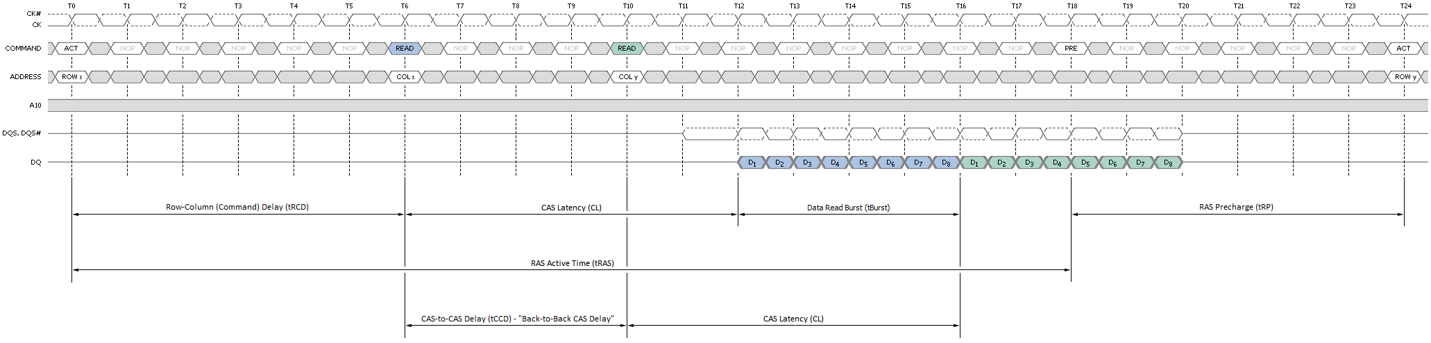
Both read and write access to DDR[3] SDRAM is burst oriented; access starts at a selected location and continues in a pre-programmed sequence for a Burst Length (BL) of 8-bits, or 1 byte, per bank. This begins with the registration of an ACT command and is followed by one or more READ or WRI commands.
Chip Select (S0#, S1#), one for each rank, either enables (LOW) or disables (HIGH) the command decoder which works like a mask to ensure commands are acted upon by the desired rank only.
The length of the each Read Burst (tBurst) is always 4 clocks (4T) as DDR memory transmits data at twice the host clock rate (4 clocks x 2 transactions/clock = 8 transactions or 8 bits per bank).
The address bits registered coincident with the ACT command are used to select the bank and page (row) to be accessed. For our hypothetical 2GB DIMM described on Page 2 of this article, Bank Selects BA0-BA2 indicate the bank and Address Input Selects A0-A13 indicate the page. Three bits are needed to uniquely address all eight banks; likewise 14 bits are needed to address all 16,384 (214) pages.
The address bits registered coincident with the READ or WRI command are used to select the targeted starting column for the burst. A0-A09 select the column starting address (210 = 1,024). A12 is also sampled during this operation to determine if a Burst Chop (BC) of 4-bits has been commanded (A12 HIGH). Even though a Burst Chop delivers only half that data of a regular Read Burst, the time period to complete the transfer is still the same: 4T. The SDRAM core simply masks the outgoing data clock strobe for the second half of the full read cycle.
During a Precharge command A10 is sampled to determine whether the precharge is intended for one bank (A10 LOW; BA selects) or all banks (A10 HIGH).
Data Input/Output pins DQ0-DQ63 provide the 64-bit wide data interface between the memory controller embedded in the CPU and each DIMM. Those with a triple-channel capable CPU, like the Intel Core i7-series processor, will come to understand why the memory bus width is reported as 192-bit – three independently operated channels each with a 64-bit interface makes 192. Those of you running a Core 2 or a Core i3/i5 will have to make do with just two channels for a total bus width of 128 bits.
Each channel can be populated with up to two DIMMs. This means there could be a maximum of four ranks per channel, assuming we install a matched pair of dual-rank modules. Installing more than one DIMM per channel does not double the Memory Bus bandwidth, as modules co-located in the same channel must compete for access to a shared 64-bit sub-bus; however, adding more modules does have the added benefit of doubling the number of pages that may be open concurrently (twice the ranks for twice the fun!).
Figure 3 attempts to provide a top-down look at the minimum cycle needed to first open a page in memory, and then read data from the activated page; Figure 4 shows the same, only from a much more fundamental perspective; and Figure 5 provides a detailed accounting of the timing involved.
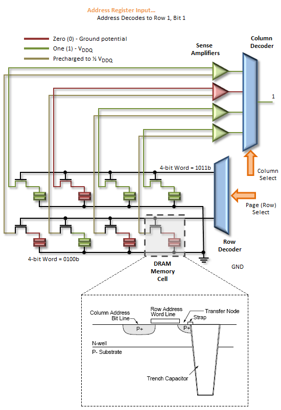
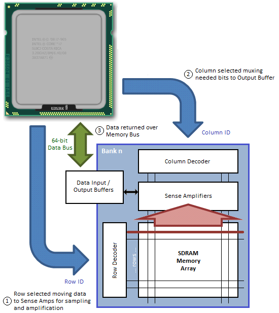
In this example we assume the bank has no open page, thus is already in the proper precharged state to support a new page access command. Step 1 selects the bank; Step 2 selects the column; and Step 3 bursts the data out over the Memory Bus. A 1-bit row address and a 2-bit column address are all we need to read any data stored in our 2 x 4-bit x 1 (bank) Memory Array.
An Activate command prompts the routing of the specified page address to be accessed to the Row Decoder where it triggers the chosen Word Line to appear at the input of the Sense Amps. As previously stated, this takes a finite time - Row-Column (or Command) Delay (tRCD) is used to program the minimum wait time the memory controller allows for this to occur before it issues the next command in the sequence. Attempting to set too low a timing can lead to inconclusive operation, often resulting in data corruption and other data access issues that ultimately lead to system crashes and other application errors.
Next, the column address provided with the Read command selects the right Bit Line, beginning the process of disregarding those bits that were not addressed. The wait associated with these events is the CAS Latency (CL or tCAS).
The Sense Amps work by sensing the direction of the voltage swing induced on the sense line when the Word Line is activated. Activating the page gates-on the switching element holding back the accumulated charge in a trench filled with dielectric material used to create the capacitive storage element of the memory cell. When this happens the sense line, starting from VRefDQ (½ VDDQ), either swings positive or negative, depending on the potential of the sampled memory cell. An increase in voltage encodes a 1, while a decrease means 0.
The Sense Amps are not comparators. Rather, each Sense Amp interfaces with a pair of memory cells, reducing the total number of amplifiers needed to otherwise sense the entire array by a factor of two.
Following the read, any charge stored in the memory cells is obliterated. This is what is meant by a destructive read: not only do the Sense Amps cache the page for access, they now hold the only known copy of that page of memory! Precharging the bank will force the Sense Amps to "write" the page back to the array and will prepare the sense lines for the next page access by "precharging" them to ½ VDDQ. This accomplishes two thing: (1) It returns all sense rails to a known, consistent potential, and (2) it sets the pre-sense line voltage at exactly half the full-scale value of VDDQ, ensuring whatever the potential stored in the cell, there will be a swing in voltage when the proper Word Line is activated.


46 Comments
View All Comments
bowhe - Tuesday, October 26, 2010 - link
Thanks for these great articles!What I didn't understand yet:
You state "Installing more than one DIMM per channel does not double the Memory Bus bandwidth, as modules co-located in the same channel must compete for access to a shared 64-bit sub-bus; however, adding more modules does have the added benefit of doubling the number of pages that may be open concurrently (twice the ranks for twice the fun!)". This sounds very positive, but:
Some system manufacturers state that with 3 dimms the memory frequency can be for example 1333MHz, but with 6 dimms it needs to drop to 800MHz. Why does the frequency need to drop when using 6 versus 3 dimms? Does this apply to high end boards like the Gigabyte-X58A-UD9?
Some manufacturer states in a small side note of a 24GB kit (6x4GB) that the stated frequency/timing is only guaranteed when using 3 dimm slots. This leads me to think that any 3 dimms of the set can do the stated timing, but when all are used something inherent in the design or interaction of the i7 processor, motherboard and dimm prevents the use of stated frequency/timings? What is it?
Can one overcome these limitations by adjusting voltages in a high end board like the Gigabyte-X58A-UD9? (without use of extreme cooling <32F/0C)
Thanks a lot!
kakfjak - Thursday, May 5, 2011 - link
www.stylishdudes.com
All kinds of shoes + tide bag
Free transport
cochleoid - Tuesday, March 12, 2013 - link
"When associated in groups of two (DDR), four (DDR2) or eight (DDR3), these banks form the next higher logical unit, known as a rank. "This mislead me. DDR2 may have coincidentally introduced 3 bit banks - allowing for 8 bank chips - but a typical old SDRAM (no DDR) chip had 4 banks.
"We can now see why the DDR3 core has a 8n-prefetch (where n refers to the number of banks per rank) as every read access to the memory requires a minimum of 64 bits (8 bytes) of data to be transferred. This is because each bank, of which there are eight for DDR3, fetches no less than 8 bits (1 byte) of data per read request - the equivalent of one column's worth of data. Whether or not the system actually makes use of all 8 bytes of transferred data is irrelevant. Any delivered data not actually requested can be safely disregarded as it's just a copy of what is still retained in memory."
This threw me off even more. What's happening is that the data at 8 consecutive (or otherwise close, depending on the burst mode) column addresses is being bursted on each read. "n" refers to the width of the memory chip, or the size of the "word" at a particular column address. "n" does not have any relation to the number of banks in a rank.
8 8bit-wide DDR3 chips would make a total module width of 64 bits or 8 bytes at each column address. 8 column addresses would be 64 bytes (not 8 bytes, as the article seems to suggest), which actually corresponds to the cacheline size on most PCs.
SDRAM could burst in sizes of 1,2,4,8
DDR could burst in sizes of only 2,4,8
DDR2 could burst in sizes of only 4,8
DDR3 can burst only in 8.
(All of these could burst in 8, filling the 64 byte cachline in one read operation. The difference with the generations of DDR has been a larger minimum wait in interface clock cycles as the interface got faster and the row accesses remained sluggish.)
The internal clock of SDRAM has been limited by the speed of row accesses. What the 2n,4n,8n prefetches are doing is transferring more of this data available in an open row out at higher interface speeds with the rest of the system. It has nothing to do with the banks.
SDRAM chips were segmented into independently operating banks so that parallel operations on interleaved banks could be synchronized or pipelined. 2n, 4n, and 8n prefetch buffering can be applied without independently operating banks.
ricardo_sa - Saturday, March 26, 2016 - link
Thanks for the detailed explanation. You really saved my day. Ive read this article some time ago to help me understand how a DDR3 worked (theres few detailed explanations on google) and it turned out to be the worst mistake possible. I got the concepts wrong because of the incompetence of the publisher and lost a lot of time dealing with that 8 Bank misconception about the 64 bits.So it turns out one can only write a burst at 1 bank at a time, am i right? Otherwise you could access all the 8 banks in one single write/read....
Huendli - Friday, March 13, 2015 - link
Thanks for this interesting read with much attention to detail!"a top priority [...] should be to focus development on reducing absolute minimum latency requirements for timings such as CAS and tRCD, rather than chasing raw synthetic bandwidth figures or setting outright frequency records at the expense of unduly high random access times."
The latter's exactly what happened. DDR3-1600 modules with CL7 timings were widely available at the time this article had been written. Nowadays, you only get ridiculously-named bars with equally-ridiculously monstrous heatspreaders, but more bandwidth and worse timings than ever.
Anuradha - Tuesday, March 9, 2021 - link
Each rank consists of 8 banks, OR, each rank consists of 8 ICs and each IC consists of 8 banks??