Intel's 50Gbps Silicon Photonics Link: The Future of Interfaces
by Brian Klug on July 30, 2010 6:49 AM EST- Posted in
- Trade Shows
- Intel
- Photonics
- Laser
It's all about Silicon
I mentioned material constraints before - without getting into too much detail, let’s talk about what makes a laser work. For every laser, you need a few things: gain medium (which should spontaneously emit photons in the presence of other photons, effectively adding optical gain), an optical resonator or feedback (in its simplest form, a cavity with mirrors at both ends), and some way of pumping (providing energy to, either electrically, optically, or whatever works for the material) the gain medium.
The problem with silicon has been that it traditionally hasn’t lent itself to creating light very well at all - it has what’s called an indirect bandgap. When electrons fall from one energy state to the other, instead of the material emitting a photon (which is what happens in a direct bandgap material), it emits primarily phonons (lattice vibrations - and through a ton of hand waving and thermodynamic processes, heat), and very few photons. In order for a material to emit large quantities photons when electrically pumped, it should have a direct bandgap.
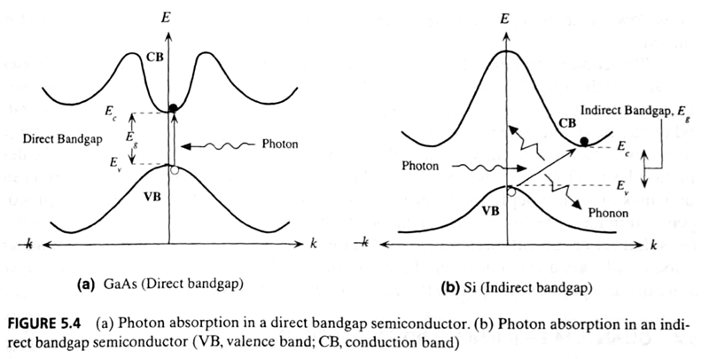
Indirect vs Direct bandgap - from Optoelectronics and Photonics: Principles and Practices by S. O. Kasap
The result for the longest time was that making a silicon laser seemed fundamentally impractical - how can something which doesn’t want to emit light be a good gain material at all?
Silicon has advantages, however. For example, silicon oxide makes an almost ideal cladding material (surrounding normal silicon). Think - fiber optic cable, but as traces embedded in your motherboard, all manufactured using traditional CMOS processes available now.
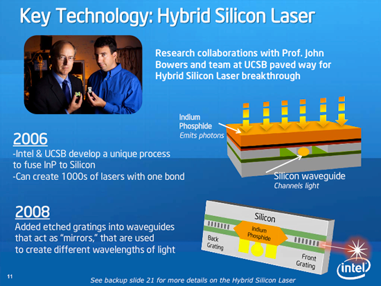
What’s new about Intel’s design - by John Bowers’ group at UCSB and a number of other researchers - is that the laser is hybrid silicon. Other previous designs have used other gain media with direct bandgaps more suitable for spontaneous emission, but with other bigger design challenges. One problem with these other materials that the crystal lattice may be too different from the silicon substrate underneath it - the result is what’s called lattice mismatch and it results in undesired optoelectronic properties. To some extent, lattice mismatch can be mitigated with an epitaxial (imagine an intermediary layer between the two mismatched material). Another problem is that thermal expansion of the materials (silicon, and whatever other material is being used for the laser) is often different as well, making it hard to physically keep things together and creating a host of other challenges. There’s also the issue of aligning the system. Previous designs have worked, at the expense of being more difficult to fabricate, and thus more expensive.

Intel’s design uses indium phosphide (InP) and aluminum gallium indium arsenide (AlGaInAs) layers, all of which can be deposited at wafer scale. The result is that there’s no discrete laser assembly or alignment. Wavelength selection and feedback are done with a distributed feedback bragg grating, which is relatively conventional. The combination of materials and manufacturing processes in this design by Intel yields itself to mass production without caveats. The end result is a hybrid silicon laser that's relatively easy to manufacture in large quantities using traditional processes.
As for the detector - bias a similar stack of components the other way, and you’re done.
Combined with Intel’s work on photonic integrated circuits on silicon for the modulator, waveguide, multiplexer and demultiplexer (for WDM), and you can see how the building blocks necessary for building optical interconnects came together.


42 Comments
View All Comments
ghot - Thursday, August 5, 2010 - link
"Blinded by the light...." I'm 53 years old and having been waiting for this since the 1st TI calculator hit the market in 1976. Unfortunately I probably won't live to see the 1st totally optical, consumer affordable PC.This doesn't prove 'Murphy's Law....it squares or even cubes it.
The best part, isn't even the speed (although it will be incredible) but rather the fact that PCB printed circuits can be a long as the design requires. Imagine a motherboard 5 inches wide and 3-4 foot tall. Then a PC enclosure could look more like a 4 foot tall 6x6 inch speaker enclosure for example.
Cooling needs will be greatly reduced as well. Just try to imagine the over clocking potential.
I used to drool over the 1st commercially available digital watch...the Pulsar....didn't even have LED's...it used tiny Nixie Tubes.....and now this.
When most of you are my age, you'll be complaining that your brand new Intel P4 (yes P4..maybe in YOUR lifetime, Intel will get back to simple naming schemes) is only capable of 4Thz on air. And, as every over clocker knows....increase the speeds in small increments...say .....10Ghz each time...lol
I am so jealous :)
ziaullahk - Sunday, February 18, 2018 - link
And to think about it, we just reached 100GBps according to https://compoundtek.com/news