Intel's 50Gbps Silicon Photonics Link: The Future of Interfaces
by Brian Klug on July 30, 2010 6:49 AM EST- Posted in
- Trade Shows
- Intel
- Photonics
- Laser
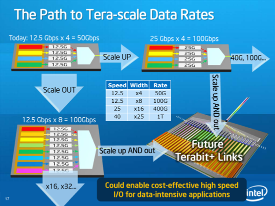
Scaling up (bitrate) and out (WDM)
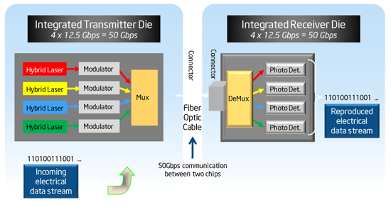
Intel demonstrated an effective speed of 12.5 gigabits/s per wavelength. Using wavelength division multiplexing (WDM), one can increase the number of wavelengths (or channels) in the fiber, effectively adding more bandwidth. Intel calls this 'scaling out.' This is what’s done in virtually every long haul fiber optic telecommunications network. Even though each wavelength in conventional teleco systems might only be 10 or 20 gigabits/s, the fiber itself can carry many wavelengths, resulting in much higher aggregate bandwidth for a single fiber.
Wavelength Division Multiplexing (WDM)
One can also increase the bitrate of each channel, intel calls this 'scaling up.'
Intel’s demonstration is effectively a vastly miniaturized end to end fiber optic telecommunications system. Instead of cities, you’ve got CPUs and ICHs. Instead of a rack of modulators and optical multiplexers, you’ve got one chip on both ends. The links between components are inevitably going optical, the same way growing need for more and more bandwidth drove almost all terrestrial communications into fiber optic networks.
Both this 50G silicon photonics link and Light Peak are at the core of Intel’s overall I/O strategy for the future, one where copper data links are supplanted almost entirely by optical fibers. No doubt copper will still live on - one still needs to bring power to devices - but in a reduced capacity.
Light Peak is what Intel is calling its first consumer implementation of an external optical bus, and will start at 10 gigabits per second, and will start appearing in products sometime in 2010. The bus will support multiple protocols as well - in theory, you could send USB, ethernet, audio, and video at super fast rates over one unified optical connection. If you think about the same thing happening but on the motherboard, you’ll get a sense for the beginning of how optical data connections will supplant copper.
Hopefully some day we’ll be talking about replacing electrons in microprocessors with photons, and computing entirely with light. Optical computing poses a host of challenges before it can be fully realized, but eventually Intel might replace ICs with photonic equivalents entirely. That future is still decades away, but until then we’ll definitely be using optical busses for moving data around.


42 Comments
View All Comments
dasHHa - Friday, July 30, 2010 - link
Moore's law still going on!Muscles - Friday, July 30, 2010 - link
A lot to look forward to in the future.DJMiggy - Friday, July 30, 2010 - link
Very good article. VERY exciting stuff. I look forward to the future. Both near and far!*sings* In the year two thousaaaaaaaaaaaaaaaaaaand!
GullLars - Wednesday, August 4, 2010 - link
*sings* In the year 2525...I just drifted off and almost drooled thinking about this combined with tiered non-uniform Solid State Storage (L1-3/4 volatile, and 4/5 none-volatile, highly parallel).
Already today you can get 100+ MB/s (read) from a single NAND chip (ONFI 2.x), so scaling out to 2^n channels you could quickly aggregate bandwidth to several GB/s for parallel workloads or bulk (>1MB) transfers, without insane costs.
With a re-make of storage management (like Fusion-IO's new "Virtual Storage Layer") and streamlining of the initiating part of program codes, you could load the operating system and any program near-instant. I've already had loading times around a second for many programs (and a few seconds for the really heavy ones) for two years now thanks to my RAIDed SSDs <3, but this would be a new level of performance.
KG Bird - Friday, July 30, 2010 - link
This was a very interesting piece and reminds me of a few things I'd stuffed into the back of my brain. Just to clear up a couple of things though...From Wikipedia: Epitaxy refers to the method of deposition a monocrystalline film on a monocrystalline substrate.
So this device is made through an epitaxial process.
Intel puts down an epitaxial buffer layer to smooth out the differences in lattices between the silicon and the next layer. If you don't use a buffer layer, you get defects such as voids or bulges that lead to the undesirable properties mentioned, or it just plain overheats at the defect location and doesn't work.
3DoubleD - Friday, July 30, 2010 - link
It is likely that the buffer layer is a metamorphic layer. The use of a quaternary alloy (AlInGaAs) alloys engineers to slowly vary the lattice constant from that of Si to that of InP. This prevents the lattice strain from ever reaching a point where it is energetically favorable to create a mismatch dislocation and thus degrading device performance. All is easier said that done and it's great that Intel was able to successfully implement this technique.Another method of integrating high performance III-V semiconductor materials onto Si are nanowires. The small nanowire diameters allows for mismatched materials to be connected without metamorphic layers.
In the next 10 years we will finally begin to leave the silicon dominated electronics industry into this hybrid type, where the superior performance of III-V semiconductors will meet the affordability and level of integration only enjoyed by the silicon community. There is no telling what this will look like, but integrated photonic circuits is just the beginning. Everything from a high mobility electron transistor to a single electron transistor would become possible on silicon in an affordable way. This will extend outside the integrated circuit world and into other areas such as solar cells, photo detectors, LEDs, biosensors, ect. We are only scratching the surface.
eanazag - Friday, July 30, 2010 - link
Good article. I am waiting for some free light Intel thingys. It happens to be 2010 now.zalves - Friday, July 30, 2010 - link
I see the future! no local storage and not even processing. Praises to the light!misterjohnnyt - Friday, July 30, 2010 - link
Maybe we can build Positronic Brains with these...Pinski - Friday, July 30, 2010 - link
So, Intel is now at 50% of what another company(Infinera) is doing. And they're doing it with 10x10Gb wavelengths. With a plan to move to 5x100Gb wavelengths by 2012.I guess, it'd be nice to have this article maybe include a comparison to what other companies are already doing or planning on doing.