Intel's 50Gbps Silicon Photonics Link: The Future of Interfaces
by Brian Klug on July 30, 2010 6:49 AM EST- Posted in
- Trade Shows
- Intel
- Photonics
- Laser
It's all about Silicon
I mentioned material constraints before - without getting into too much detail, let’s talk about what makes a laser work. For every laser, you need a few things: gain medium (which should spontaneously emit photons in the presence of other photons, effectively adding optical gain), an optical resonator or feedback (in its simplest form, a cavity with mirrors at both ends), and some way of pumping (providing energy to, either electrically, optically, or whatever works for the material) the gain medium.
The problem with silicon has been that it traditionally hasn’t lent itself to creating light very well at all - it has what’s called an indirect bandgap. When electrons fall from one energy state to the other, instead of the material emitting a photon (which is what happens in a direct bandgap material), it emits primarily phonons (lattice vibrations - and through a ton of hand waving and thermodynamic processes, heat), and very few photons. In order for a material to emit large quantities photons when electrically pumped, it should have a direct bandgap.
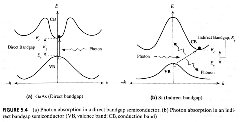
Indirect vs Direct bandgap - from Optoelectronics and Photonics: Principles and Practices by S. O. Kasap
The result for the longest time was that making a silicon laser seemed fundamentally impractical - how can something which doesn’t want to emit light be a good gain material at all?
Silicon has advantages, however. For example, silicon oxide makes an almost ideal cladding material (surrounding normal silicon). Think - fiber optic cable, but as traces embedded in your motherboard, all manufactured using traditional CMOS processes available now.
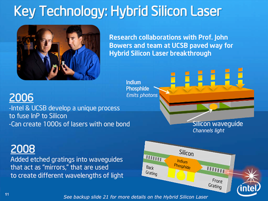
What’s new about Intel’s design - by John Bowers’ group at UCSB and a number of other researchers - is that the laser is hybrid silicon. Other previous designs have used other gain media with direct bandgaps more suitable for spontaneous emission, but with other bigger design challenges. One problem with these other materials that the crystal lattice may be too different from the silicon substrate underneath it - the result is what’s called lattice mismatch and it results in undesired optoelectronic properties. To some extent, lattice mismatch can be mitigated with an epitaxial (imagine an intermediary layer between the two mismatched material). Another problem is that thermal expansion of the materials (silicon, and whatever other material is being used for the laser) is often different as well, making it hard to physically keep things together and creating a host of other challenges. There’s also the issue of aligning the system. Previous designs have worked, at the expense of being more difficult to fabricate, and thus more expensive.

Intel’s design uses indium phosphide (InP) and aluminum gallium indium arsenide (AlGaInAs) layers, all of which can be deposited at wafer scale. The result is that there’s no discrete laser assembly or alignment. Wavelength selection and feedback are done with a distributed feedback bragg grating, which is relatively conventional. The combination of materials and manufacturing processes in this design by Intel yields itself to mass production without caveats. The end result is a hybrid silicon laser that's relatively easy to manufacture in large quantities using traditional processes.
As for the detector - bias a similar stack of components the other way, and you’re done.
Combined with Intel’s work on photonic integrated circuits on silicon for the modulator, waveguide, multiplexer and demultiplexer (for WDM), and you can see how the building blocks necessary for building optical interconnects came together.


42 Comments
View All Comments
DanNeely - Friday, July 30, 2010 - link
I guess, it'd be nice to have this comment maybe include a citation to what other companies are already doing or planning on doing.Huron80 - Friday, July 30, 2010 - link
Look at Infinera, aren't they a networking provider?As stated in the article, Intel is taking what is being done effectively in Fiber Optic network transmissions - the same ones that help connect the internet - and are making a miniature version that will work inside your computer - the connections on the motherboard to components.
has407 - Friday, July 30, 2010 - link
Infinera's achievements are nothing to sneeze at, but they're quite different. AFAIK Infinera still uses a separate process for the optical components (the PIC, or "photonics IC"); they don't put everything on a single die. That's fine for certain markets, and they seem to have done well with Telecoms. However, for large scale low cost production; you're very unlikely to see it replace inter-chip or intra-chip interconnects in volume markets.Luxera is probably closer to what Intel is showing. They partnered with Freescale to integrate the photonics and electronics fab in CMOS last year to allow "low cost high volume" production"; exactly what may come from that is TBD. While we haven't seen much, Luxera's Blazar "Optical Active Cable" is a clue. But again, that's targeted at external inter-system connections; hard to tell if that's due to technology imitations or if Luxera is simply trying to generate revenue and build a market based on the technology is unclear.
In short, it's all about being able to produce everything--optical and electronic components--using a common and low cost fab. In that, Luxera/Freescale and Intel seem to be in the lead, and I'd wager Intel is most likely to bring it mainstream sooner rather than later.
This has the potential to significantly reduce the "interconnect tax" imposed by copper, which increases as speeds increase, and will soon be untenable. Intel said 20GHz was the ceiling for serial interconnects some years ago. (Teething problems related to power consumption with 10Gbe copper provide clues.) Even Inte's prediction is off by a factor of two, the end of that road is in sight.
At a guess, we'll see photonics integration in high-margin parts with the first replacing QPI as the backbone interconnect in high-end systems. Or maybe blade systems with optical backplanes. Or...
Jaybus - Friday, July 30, 2010 - link
Another thing to consider is that one reason for motherboards being as large as they are is that there must be hundreds of traces interconnecting components. Components have to be spread out to leave room for the traces. This technology will allow for one optical link to replace all of the myriad traces connecting the CPU to the northbridge, for example. Components can be closer together.Another factor is bus cards. Cards can be placed anywhere and connected by a single small fiber optic cable. Disk drives, etc. can be connected optically. This will substantially reduce the size of a full featured motherboard.
arnavvdesai - Friday, July 30, 2010 - link
While I agree components can be closer. We also have to think about the issue of heat dissipation. If we start moving items closer then we might have to deal with other issues.Jaybus - Monday, August 2, 2010 - link
Certainly, cooling will force a minimum size, but there is no reason an ATX board could not be shrunk to ITX size, at least, yet have even more i/o capability than a current ATX board. The board components could be placed as closely as is feasible, given the heat dissipation required.clarkn0va - Tuesday, August 3, 2010 - link
Doesn't replacing electrons with photons reduce the amount of heat produced?GullLars - Wednesday, August 4, 2010 - link
Not necessarily, you still need energy converting the digital electronic signal to optical and back, it's just the transport that saves energy, and only as much as the resistance in the copper wire. For high frequency or long distance information transport, it can be noticeable power savings.Regarding cooling, one quick solution is to switch the default from air cooling to liquid cooling in higher power systems. By placing the radiator, pump, and reservoir outside the system, and exploiting the new available dimension inside the case, you can make much smaller (and quieter while better cooled) systems.
Ninhalem - Friday, July 30, 2010 - link
The problem with a shrinking motherboard is that would leave too little room to put in cooling for the CPU and the memory. We're still a ways away from having CPUs running on light like the article said. I'm interested in not only shrinking the board a bit but having a different shape and orientation for the memory, video, audio card, and any other component you have in the case.Maybe have an upside down L shaped board where you can place the SATA II ports close to the hard drives and the optical drive. Maybe a start shaped board. Now that distance doesn't matter, the possibilities are endless. Very fascinating and exciting stuff.
darckhart - Friday, July 30, 2010 - link
sure, but they haven't talked about heat constraints yet.