NVIDIA’s GeForce GTX 480 and GTX 470: 6 Months Late, Was It Worth the Wait?
by Ryan Smith on March 26, 2010 7:00 PM EST- Posted in
- GPUs
The GF100 Recap
NVIDIA first unveiled its GF100 (then called Fermi) architecture last September. If you've read our Fermi and GF100 architecture articles, you can skip this part. Otherwise, here's a quick refresher on how this clock ticks.
First, let’s refresh the basics. NVIDIA’s GeForce GTX 480 and 470 are based on the GF100 chip, the gaming version of what was originally introduced last September as Fermi. GF100 goes into GeForces and Fermi goes into Tesla cards. But fundamentally the two chips are the same.
At a high level, GF100 just looks like a bigger GT200, however a lot has changed. It starts at the front end. Prior to GF100 NVIDIA had a large unified front end that handled all thread scheduling for the chip, setup, rasterization and z-culling. Here’s the diagram we made for GT200 showing that:
NVIDIA's GT200
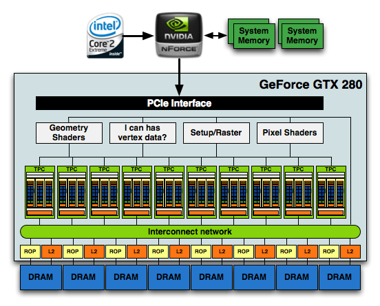
The grey boxes up top were shared by all of the compute clusters in the chip below. In GF100, the majority of that unified front end is chopped up and moved further down the pipeline. With the exception of the thread scheduling engine, everything else decreases in size, increases in quantity and moves down closer to the execution hardware. It makes sense. The larger these chips get, the harder it is to have big unified blocks feeding everything.
In the old days NVIDIA took a bunch of cores, gave them a cache, some shared memory and a couple of special function units and called the whole construct a Streaming Multiprocessor (SM). The GT200 took three of these SMs, added texture units and an L1 texture cache (as well as some scheduling hardware) and called it a Texture/Processor Cluster. The old GeForce GTX 280 had 10 of these TPCs and that’s what made up the execution engine of the GPU.
NVIDIA's GF100

Click to Enlarge
With GF100, the TPC is gone. It’s now a Graphics Processing Cluster (GPC) and is made up of much larger SMs. Each SM now has 32 cores and there are four SMs per GPC. Each GPC gets its own raster engine, instead of the entire chip sharing a larger front end. There are four GPCs on a GF100 (however no GF100 shipping today has all SMs enabled in order to improve yield).

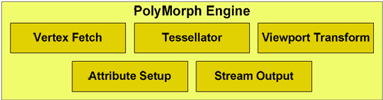
Each SM also has what NVIDIA is calling a PolyMorph engine. This engine is responsible for all geometry execution and hardware tessellation, something NVIDIA expects to be well used in DX11 and future games. NV30 (GeForce FX 5800) and GT200 (GeForce GTX 280), the geometry performance of NVIDIA’s hardware only increases roughly 3x in performance. Meanwhile the shader performance of their cards increased by over 150x. Compared just to GT200, GF100 has 8x the geometry performance of GT200, and NVIDIA tells us this is something they have measured in their labs. This is where NVIDIA hopes to have the advantage over AMD, assuming game developers do scale up geometry and tessellation use as much as NVIDIA is counting on.
NVIDIA also clocks the chip much differently than before. In the GT200 days we had a core clock, a shader clock and a memory clock. The core clock is almost completely out of the picture now. Only the ROPs and L2 cache operate on a separate clock domain. Everything else runs at a derivative of the shader clock. The execution hardware runs at the full shader clock speed, while the texture units, PolyMorph and Raster engines all run at 1/2 shader clock speed.
Cores and Memory
While we’re looking at GF100 today through gaming colored glasses, NVIDIA is also trying to build an army of GPU compute cards. In serving that master, the GF100’s architecture also differs tremendously from its predecessors.
All of the processing done at the core level is now to IEEE spec. That’s IEEE-754 2008 for floating point math (same as RV870/5870) and full 32-bit for integers. In the past 32-bit integer multiplies had to be emulated, the hardware could only do 24-bit integer muls. That silliness is now gone. Fused Multiply Add is also included. The goal was to avoid doing any cheesy tricks to implement math. Everything should be industry standards compliant and give you the results that you’d expect. Double precision floating point (FP64) performance is improved tremendously. Peak 64-bit FP execution rate is now 1/2 of 32-bit FP, it used to be 1/8 (AMD's is 1/5).

GT200 SM
In addition to the cores, each SM has a Special Function Unit (SFU) used for transcendental math and interpolation. In GT200 this SFU had two pipelines, in GF100 it has four. While NVIDIA increased general math horsepower by 4x per SM, SFU resources only doubled. The infamous missing MUL has been pulled out of the SFU, we shouldn’t have to quote peak single and dual-issue arithmetic rates any longer for NVIDIA GPUs.

GF100 SM
NVIDIA’s GT200 had a 16KB shared memory in each SM. This didn’t function as a cache, it was software managed memory. GF100 increases the size to 64KB but it can operate as a real L1 cache now. In order to maintain compatibility with CUDA applications written for G80/GT200 the 64KB can be configured as 16/48 or 48/16 shared memory/L1 cache. GT200 did have a 12KB L1 texture cache but that was mostly useless for CUDA applications. That cache still remains intact for graphics operations. All four GPCs share a large 768KB L2 cache.

Each SM has four texture units, each capable of 1 texture address and 4 texture sample ops. We have more texture sampling units but fewer texture addressing units in GF100 vs. GT200. All texture hardware runs at 1/2 shader clock and not core clock.
| NVIDIA Architecture Comparison | G80 | G92 | GT200 | GF100 | GF100 Full* |
| Streaming Processors per TPC/GPC | 16 | 16 | 24 | 128 | 128 |
| Texture Address Units per TPC/GPC | 4 | 8 | 8 | 16 | 16 |
| Texture Filtering Units per TPC/GPC | 8 | 8 | 8 | 64 | 64 |
| Total SPs | 128 | 128 | 240 | 480 | 512 |
| Total Texture Address Units | 32 | 64 | 80 | 60 | 64 |
| Total Texture Filtering Units | 64 | 64 | 80 | 240 | 256 |
Last but not least, this brings us to the ROPs. The ROPs have been reorganized, there are now 48 of them in 6 parttions of 8, and a 64bit memory channel serving each partition. The ROPs now share the L2 cache with the rest of GF100, while under GT200 they had their own L2 cache. Each ROP can do 1 regular 32bit pixel per clock, 1 FP16 pixel over 2 clocks, or 1 FP32 pixel over 4 clocks, giving the GF100 the ability to retire 48 regular pixels per clock. The ROPs are clocked together with the L2 cache.
Threads and Scheduling
While NVIDIA’s G80 didn’t start out as a compute chip, GF100/Fermi were clearly built with general purpose compute in mind from the start. Previous architectures required that all SMs in the chip worked on the same kernel (function/program/loop) at the same time. If the kernel wasn’t wide enough to occupy all execution hardware, that hardware went idle, and efficiency dropped as a result. Remember these chips are only powerful when they’re operating near 100% utilization.
In this generation the scheduler can execute threads from multiple kernels in parallel, which allowed NVIDIA to scale the number of cores in the chip without decreasing efficiency.
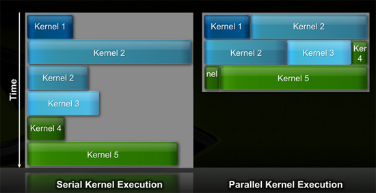
GT200 (left) vs. GF100 (right)
With a more compute leaning focus, GF100 also improves switch time between GPU and CUDA mode by a factor of 10x. It’s now fast enough to switch back and forth between modes multiple times within a single frame, which should allow for more elaborate GPU accelerated physics.
NVIDIA’s GT200 was a thread monster. The chip supported over 30,000 threads in flight. With GF100, NVIDIA scaled that number down to roughly 24K as it found that the chips weren’t thread bound but rather memory bound. In order to accommodate the larger shared memory per SM, max thread count went down.
| GF100 | GT200 | G80 | |
| Max Threads in Flight | 24576 | 30720 | 12288 |
NVIDIA groups 32 threads into a unit called a warp (taken from the looming term warp, referring to a group of parallel threads). In GT200 and G80, half of a warp was issued to an SM every clock cycle. In other words, it takes two clocks to issue a full 32 threads to a single SM.
In previous architectures, the SM dispatch logic was closely coupled to the execution hardware. If you sent threads to the SFU, the entire SM couldn't issue new instructions until those instructions were done executing. If the only execution units in use were in your SFUs, the vast majority of your SM in GT200/G80 went unused. That's terrible for efficiency.
Fermi fixes this. There are two independent dispatch units at the front end of each SM in Fermi. These units are completely decoupled from the rest of the SM. Each dispatch unit can select and issue half of a warp every clock cycle. The threads can be from different warps in order to optimize the chance of finding independent operations.
There's a full crossbar between the dispatch units and the execution hardware in the SM. Each unit can dispatch threads to any group of units within the SM (with some limitations).
The inflexibility of NVIDIA's threading architecture is that every thread in the warp must be executing the same instruction at the same time. If they are, then you get full utilization of your resources. If they aren't, then some units go idle.
A single SM can execute:
| GF100 | FP32 | FP64 | INT | SFU | LD/ST |
| Ops per clock | 32 | 16 | 32 | 4 | 16 |
If you're executing FP64 instructions the entire SM can only run at 16 ops per clock. You can't dual issue FP64 and SFU operations.
The good news is that the SFU doesn't tie up the entire SM anymore. One dispatch unit can send 16 threads to the array of cores, while another can send 16 threads to the SFU. After two clocks, the dispatchers are free to send another pair of half-warps out again. As I mentioned before, in GT200/G80 the entire SM was tied up for a full 8 cycles after an SFU issue.
The flexibility is nice, or rather, the inflexibility of GT200/G80 was horrible for efficiency and Fermi fixes that.


196 Comments
View All Comments
Ryan Smith - Wednesday, March 31, 2010 - link
My master copies are labeled the same, but after looking at the pictures I agree with you; something must have gotten switched. I'll go flip things. Thanks.Wesgoood - Wednesday, March 31, 2010 - link
Correction, Nvidia retained their crown on Anandtech. Even though some resolutions even on here were favored to ATI(mostly the higher ones). On Toms Hardware 5870 pretty much beat GTX 480 from 1900x1200 to 2560x1600, not every time in 1900 but pretty much every single time in 2560.That ...is where the crown is, in the best of the best situations, not ....OMG it beat it in 1680 ...THAT HAS TO BE THE BEST!
Plus the power hungry state of this card is just appauling. Nvidia have shown they can't compete with proper technology, rather having to just cram everything they can onto a chip and prey it works right.
Where as ATI's GPU is designed perfectly to where they have plenty of room to almost double the size of the 5870.
efeman - Wednesday, March 31, 2010 - link
I copied this over from a comment I made on a blog post.I've been with nVidia for the past decade. My brother built his desktop way back when with the Ti 4200, I bought a prefab with a 5950 ultra, my last budget build had an 8600 GTS in it, and I upgraded to the GTX 275 last year. I am in no way a fanboy, nVidia just has treated me very well. If I had made that last decision a few months later after the price hike, it would've definitely been the HD 4890; almost identical performance for ballpark $100 less.
I recently built a new high-end rig (Core i7 and all), but I waited out on dropping the money on a 5800 series card. I knew nVidia's new cards were on the way, and I was excited and willing to wait it out; I expected a lot out of them.
Now that they're are out in the open, I have to say I'm a little shaken. In many cases, the performance of the cards are not where I would've hoped they be (the general consensus seems to be 5-10% increase in performance over their ATI counterparts; I see that failing in many cases, however). It seems like the effort that nVidia put into the cards gave them lots of potential, but most of it is wasted.
"The future of PC gaming" is right in the title of this post, and that's what these cards have been built for. Nvidia has a strong lead over ATI in compute and tessellation performance now, that's obvious; however, that will only provide useful if and when developers decide to put the extra effort into taking advantage of those technologies. Nvidia is gambling right now; it has already given ATI a half-year lead on the DX11 market, and it's pushing cards that won't be fully utilized until who-knows-when (there's no telling when these technologies will be more widely integrated into the gaming market). What will it do in the meantime? ATI is already on it's way to producing its 5000-series refresh; and this time it knows the competition's performance.
I was hoping for the GTX 400s to do the same thing that the GTX 200s did: give nVidia back the high-end performance throne. ATI is not only competitive with it's counterparts, but it still has the 5970 for the enthusiast performance crown (don't forget Eyefinity!). I think nVidia made a mistake in putting so much focus into compute and tessellation performance; it would've been smarter to produce cards with similar die sizes (crappy wafer yields, anyone?), faster raw performance with tessellation/compute as a secondary objective, and more competitive pricing. It wouldn't have been a bad option to create a separate chip for the Tesla cards, one that focused on the compute performance while the GeForce cards focused on the rest.
I still have faith. Maybe nVidia will work wonders with the drivers and producing performance we were waiting for. Maybe it has something awesome brewing deep within its labs. Or maybe my fears will embody themselves, and nVidia is crossing its fingers and hoping for its tessellation/compute performance to give it the market share later on. If so, ATI will provide me with my pair of cards.
That was quite the rant; I wasn't planning on writing that much when I decided to comment on Drew Henry's (nVidia GM) blog post. I suppose I'm passionate about this sort of thing, and I really hope nVidia doesn't lose me after all this time.
Kevinmbaron - Wednesday, March 31, 2010 - link
The fact that this card comes out a year and a 1/2 after the the GTX 295 makes me sick. Add to that the fact that the GTX 295 actually is faster then the GTX 480 in a few benchmarks and very close in others is like a bad dream for nvidia. Forget if they can beat AMD, they can't even beat themselves. They could have did a die shrink on the GTX 295, add some more shadders and double the memory and had that card out a year ago and it would have crushed anything on the market. Instead they risked it all on a hair brained new card. I am a GTX 295 owner. Apperently my card is a all arround better card being it doesnt lag in some games like the 480 does. I guess i will stick with my old GTX 295 for another year. Maybe then there might be a card worth buying. Even the ATI 5970 doesn't have enough juice to justify a new purchase from me. This should be considered horrible news for Nvidia. They should be ashammed of themselves and the CEO should be asked to step down.ol1bit - Thursday, April 1, 2010 - link
I just snagged a 5870 gen 2 I think (XFX) from NewEgg.They have been hard to find in stock, and they are out again.
I think many were waiting to see if the GF100 was a cruel joke or not. I am sorry for Nivida, but love the completion. I hope Nvidia will survive.
I'll bet they are burning the midnight oil for gen 2 of the GF100.
bala_gamer - Friday, April 2, 2010 - link
Did you guys recieve the GTX480 earlier than other reviewers? There were 17 cards tested on 3 drivers and i am assuming tests were done multiple times per game to get an average. installing, reinstalling drivers, etc 10.3 catalyst drivers came out week of march 18.Do you guys have multiple computers benchmarking at the same time? I just cannot imagine how the tests were all done within the time frame.
Ryan Smith - Sunday, April 4, 2010 - link
Our cards arrived on Friday the 19th, and in reality we didn't start real benchmarking until Saturday. So all of that was done in roughly a 5 day span. In true AnandTech tradition, there wasn't much sleep to be had that week. ;-)mrbig1225 - Tuesday, April 6, 2010 - link
I felt compelled to say a few things about nvidia’s Fermi (480/470 GTX). I like to always start out by saying…let’s take the fanboyism out of the equation and look at the facts. I am a huge nvidia fan, however they dropped the ball big time. They are selling people on ONE aspect of DX11 (tessellation) and that’s really the only thing there cards does well but it’s not an efficient design. What people aren’t looking at is that their tessellation is done by the polymorh engine which ties directly into the cuda cores, meaning the more cuda cores occupied by shaders processing…etc the less tessellation performance and vice versa = less frames per sec. As you noticed we see tons of tessellation benchmarks that show the gtx 480 is substantially faster at tessellation, I agree when the conditions suite that type of architecture (and there isn’t a lot of other things going on). We know that the gf100(480/470gtx) is a computing beast, but I don’t believe that will equate to overall gaming performance. The facts are this gpu is huge (3billion + transistors), creates a boat load of heat, and sucks up more power than any of the latest dual gpu cards (295gtx, 5970) came to market 6 months late and is only faster than its single gpu competition by 10-15% and some of us are happy? Oh that’s right it will be faster in the future when dx11 is relevant…I don’t think so for a few reasons but ill name two. If you look at the current crop of dx11 games, the benchmarks and actual dx11 game benchmarks (shaders and tessellation…etc) shows something completely different. I think if tessellation was nvidia’s trump card in games then basically the 5800 series would be beat substantially in any dx11 title with tessellation turned on…we aren’t seeing that(we are seeing the opposite in some circumstances), I don’t think we will. I also am fully aware that tessellation is scalable, but that brings me to another point. I know many of you will say that it is only in extreme tessellation environments that we really start to see the nvidias card take off. Well if you agree with that statement then you will see that nvidia has another issue. The 1st is the way they implement tessellation in their cards (not very scalable imo) 2nd is, the video card industry sales are not comprised of high end gpus, but the cheaper mainstream ones. Since nvidia polymorph engine is tied directly to its shaders…u kinda see where this is going, basicly less powerful cards will be bottlenecked by their lack of shaders for tessellation and vice versa. Developers want to make money, the way they make money is selling lots of games, example crysis was a big game, however it didn’t break any records sales…truth of the matter is most people systems couldn’t run crysis. Now you look at valve software and a lot of their titles sale well because of how friendly it is to mainstream gpus(not the only thing but it does help). The hardware has to be there to support a large # of game sales, meaning that if the majority of parts cannot do extreme levels of tessellation then you will find few games to implement it. Food for thought… can anyone show me a dx11 title that the gtx480 handily beats the 5870 by the same amount that it does in the heaven benchmark or even close to that. I think as a few of you have said, it will come down to what game work better with what architecture..some will benefit nvidia(Farcry2..good example) others Ati (Stalker)…I think that is what we are seeing now. IMOP.S. I think also why people are pissed is because this card was stated to be 60% faster than the 5870. As u can see its not!!
houkouonchi - Thursday, April 8, 2010 - link
Why the hell are the screenshots showing off the AA results in a lossy JPEG format instead of PNG like pretty much anything else?dzmcm - Monday, April 12, 2010 - link
I'm not familiar with Battleforge firsthand, but I understood it uses HD Ambient Occlusion wich is a variation of Screen Space Ambient Occlusion that includes normal maps. And since it's inception in Crysis SSAO has stood for Screen Space AO. So why is it called Self Shadow AO in this article?Bit-tech refers to Stalker:CoP's SSAO as "Soft Shadow." That I'm willing to dismiss. But I think they're wrong.
Am I'm falling behind with my jargon, or are you guys not bothering to keep up?