The RV870 Story: AMD Showing up to the Fight
by Anand Lal Shimpi on February 14, 2010 12:00 AM EST- Posted in
- GPUs
Process vs. Architecture: The Difference Between ATI and NVIDIA
Ever since NV30 (GeForce FX), NVIDIA hasn’t been first to transition to any new manufacturing process. Instead of dedicating engineers to process technology, NVIDIA chooses to put more of its resources into architecture design. The flipside is true at ATI. ATI is much less afraid of new process nodes and thus devotes more engineering resources to manufacturing. Neither approach is the right one, they both have their tradeoffs.
NVIDIA’s approach means that on a mature process, it can execute frustratingly well. It also means that between major process boundaries (e.g. 55nm to 40nm), NVIDIA won’t be as competitive so it needs to spend more time to make its architecture more competitive. And you can do a lot with just architecture alone. Most of the effort put into RV770 was architecture and look at what it gave ATI compared to the RV670.
NVIDIA has historically believed it should let ATI take all of the risk jumping to a new process. Once the process is mature, NVIDIA would switch over. That’s great for NVIDIA, but it does mean that when it comes to jumping to a brand new process - ATI has more experience. Because ATI puts itself in this situation of having to jump to an unproven process earlier than its competitor, ATI has to dedicate more engineers to process technology in order to mitigate the risk.
In talking to me Carrell was quick to point out that moving between manufacturing processes is not a transition. A transition implies a smooth gradient from one technology to another. But moving between any major transistor nodes (e.g. 55nm to 45nm, not 90nm to 80nm) it’s less of a transition and more of a jump. You try to prepare for the jump, you try your best to land exactly where you want to, but once your feet leave the ground there’s very little to control where you end up.
Any process node jump involves a great deal of risk. The trick as a semiconductor manufacturer is how you minimize that risk.
At some point, both manufacturers have to build chips on a new process node otherwise they run the risk of becoming obsolete. If you’re more than one process generation behind, it’s game over for you. The question is, what type of chip do you build on a brand new process?
There are two schools of thought here: big jump or little jump. The size refers to the size of the chip you’re using in the jump.
Proponents of the little jump believe the following. In a new process, the defect density (number of defects per unit area on the wafer) isn’t very good. You’ll have a high number defects spread out all over the wafer. In order to minimize the impact of high defect density, you should use a little die.
If we have a wafer that has 100 defects across the surface of the wafer and can fit 1000 die on the wafer, the chance that any one die will be hit with a defect is only 10%.
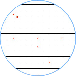
A hypothetical wafer with 7 defects and a small die. Individual die are less likely to be impacted by defects.
The big jump is naturally the opposite. You use a big die on the new process. Now instead of 1000 die sharing 100 defects, you might only have 200 die sharing 100 defects. If there’s an even distribution of defects (which isn’t how it works), the chance of a die being hit with a defect is now 50%.
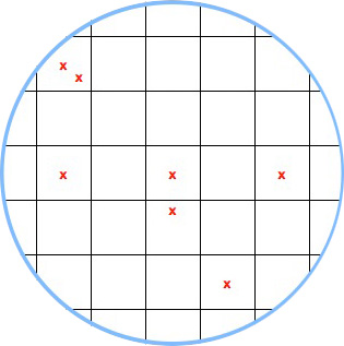
A hypothetical wafer with 7 defects and a large die.
Based on yields alone, there’s no reason you’d ever want to do a big jump. But there is good to be had from the big jump approach.
The obvious reason to do a big jump is if the things you’re going to be able to do by making huge chips (e.g. outperform the competition) will net you more revenue than if you had more of a smaller chip.
The not so obvious, but even more important reason to do a big jump is actually the reason most don’t like the big jump philosophy. Larger die are more likely to expose process problems because they will fail more often. With more opportunity to fail, you get more opportunity to see shortcomings in the process early on.
This is risky to your product, but it gives you a lot of learning that you can then use for future products based on the same process.


132 Comments
View All Comments
devene - Sunday, February 14, 2010 - link
Just like many others, I've been a long time reader and I just couldn't carry on without leaving a comment:This has been an article, just like the RV770 one. It may not reveal many facts but is tremendously insightful and inspiring. Thank you for bringing this deeply hidden information out to the public and to the "fans". Please do everything in your power to continue this trend.
Once again, thank you Anand,
devene
medi01 - Sunday, February 14, 2010 - link
Germans say "lange Rede kurzer Sinn". So many pointless sentences that do not tell anything even remotely interesting.TGressus - Sunday, February 14, 2010 - link
Even the home team could not be sold on Eyefinity...William Gaatjes - Sunday, February 14, 2010 - link
Fantastic article."
First, it massively increased the confidence level of the engineering team. There’s this whole human nature aspect to everything in life, it comes with being human. Lose confidence and execution sucks, but if you are working towards a realistic set of goals then morale and confidence are both high. The side effect is that a passionate engineer will also work to try and beat those goals.
"
Finally, someone accepting and using human nature.
And see it works out...
The fun part is that a requested functionality that is desired but can not make it within the expected timeframe, can still be worked on and can be ready for the next "bulge" in the market. This way you relieve your engineers form stress, you have the time to sort errors and bugs out, you have time to solve unforseen consequences that always happen( people can get sick, a bug in software, machines breaking down) and you have a feature for the market department to market to the consumer for the next iteration of the product. This way you can use the free market to build an in the end perfect device. It is all about balance. If you have to invest to much energy in situation a, you will have less energy for situation b in a certain timeframe. We are bound by laws of nature meaning there is no "perpetuum mobile" in this universe. Nothing comes for free...
aegisofrime - Sunday, February 14, 2010 - link
Anand, you have taken an article that is really technical in nature, and turned it into something entertaining to read and yet informative for non-engineer types. My hats off to you. This is really the right balance of information and readability. If only all the Scientific Papers I have to read were written like this!dukeariochofchaos - Sunday, February 14, 2010 - link
i wonder if you will give fermi the same drama queen touch?i hope so.
Jamahl - Sunday, February 14, 2010 - link
I don't think anyone wants to read nvidia's marketing department tell us how awesome PhysX and CUDA is again tbh.TGressus - Sunday, February 14, 2010 - link
I suspect Fermi will be able to stand on it's technological innovation.RJohnson - Sunday, February 14, 2010 - link
...and it's exorbitant price/die size will exclude mere mortals from owning one.Spoelie - Sunday, February 14, 2010 - link
That depends entirely on the openness of NVIDIA on the subject, historically not one of their strong points.In fact ATi's take on NVIDIA's design process has been more informative than what has come out of NVIDIA itself.
But here's to hoping..