New Westmere Details Emerge: Power Efficiency and 4/6 Core Plans
by Anand Lal Shimpi on February 3, 2010 12:00 AM EST- Posted in
- CPUs
Today Intel started talking about its ISSCC plans and included in the conference call were some details on Westmere that I previously didn't know. Most of it has to do with power savings, but also some talk about 32nm quad-core Westmere derivatives!
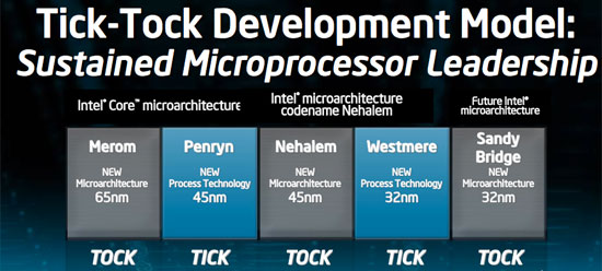
Westmere is Intel’s 32nm Nehalem derivative. Take Nehalem with all of its inherent goodness, add AES instructions, build it using 32nm transistors and you’ve got Westmere.
Westmere's Secret: Power Gated Un-Core
We just recently met the first incarnation of Westmere - Clarkdale, the dual-core processor that’s been branded the Core i3 and Core i5. Later this quarter we’ll meet Gulftown, a six-core Westmere that’ll be sold under the Core i7 label. All of that is old news, now for the new stuff.
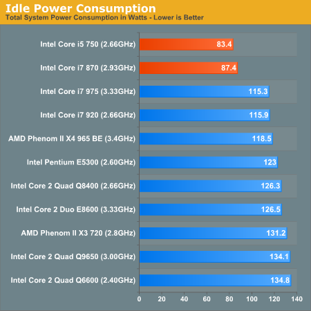
With Nehalem Intel started power gating parts of the chip. Stick a power gate transistor in front of the supply voltage to each core and you can effectively shut off power (including leakage power) to the core when it’s not in use. This was a huge step in increasing power efficiency, something that’s evident when you look at Nehalem idle power numbers.
When you shut off a core you need to save the core’s state so that when it wakes back up it knows what to do next. Remember that power down these cores can happen dozens of times in the course of a second. The cores can’t wake up in a reboot state, they need to simply shut off when they’re not needed and wake back up to continue work when they are needed.
In Nehalem the core’s state (what instruction it’s going to work on next, data in its registers, etc...) is saved in the last level cache - L3. Unfortunately this means that the L3 cache can’t be powered down when the cores are idle, because that’s where they store their state information. Take this one step further and it also means that Nehalem’s L3 cache wasn’t power-gated.
In Westmere, Intel has added a dedicated SRAM to store core state data. Each core dumps its state information into the dedicated SRAM and then shuts off. With the state data kept out of the L3 cache, Westmere takes the next logical step and power gates the L3.
Intel lists this dedicated SRAM as a Westmere-mobile feature, there’s a chance it’s not present on the desktop chips. But it makes sense. Without a way of powering down the L3 cache, Westmere would be a very power hungry mobile CPU. Westmere appears to make it mobile-friendly.
Hex and Quad Core Westmere in 2010?
The last bits of information Intel revealed have to do with its high end desktop/workstation/server intentions with Westmere. The 6-core Westmere is a 240mm^2 chip made up of 1.17B transistors:
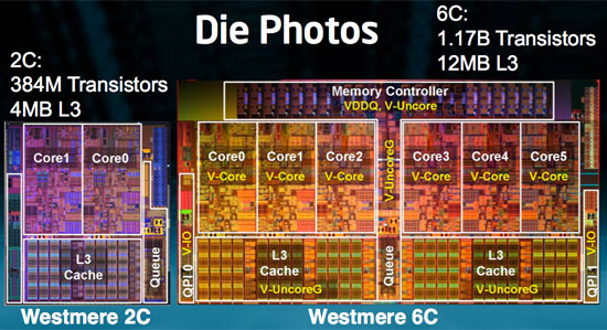
That’s six cores on a single die, but with 12MB of L3 cache. Remember that Nehalem/Lynnfield have 8MB and Clarkdale has 4MB. Nehalem’s chief architect, Ronak Singhal told me that he wanted to maintain at least 2MB of L3 per core on the die. A 6-core Westmere adheres to that policy.
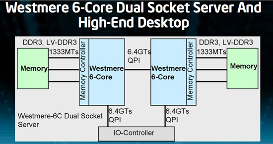
The chip works in existing LGA-1366 sockets, so you still have three DDR3 memory channels. 6C Westmere does support both regular DDR3 (1.5V) as well as low voltage DDR3 (1.35V). This is particularly useful in servers where you’ve got a lot of memory present, power consumption should be noticeably lower.
The other big news is that Intel will be releasing 4-core variants of Westmere as well. While I originally assumed this would mean desktop and server, Intel hasn't committed to anything other than a quad-core Westmere. These parts could end up as server only or server and desktop.
The table below shows you the beauty of 32nm. Smaller die, more transistors:
| CPU | Codename | Manufacturing Process | Cores | Transistor Count | Die Size |
| Westmere 6C | Gulftown | 32nm | 6 | 1.17B | 240mm2 |
| Nehalem 4C | Bloomfield | 45nm | 4 | 731M | 263mm2 |
| Nehalem 4C | Lynnfield | 45nm | 4 | 774M | 296mm2 |
| Westmere 2C | Clarkdale | 32nm | 2 | 384M | 81mm2 |
It also shows that there's a definite need for Intel to build a quad-core 32nm chip. Die sizes nearing 300mm2 aren't very desirable. The question is whether we'll see quad-core 32nm in 2010 desktops or if we'll have to wait for Sandy Bridge in 2011 for that.
We’ll find out soon enough.


45 Comments
View All Comments
Inspector2211 - Wednesday, February 3, 2010 - link
Hmmm.AMD is about a year behind Intel with respect to process technology, and Intel just introduced 32nm processors this January.
Judging from that, it is very likely that AMD will introduce 32nm processors in Q1/2011, and since quad core processors seem to be their bread and butter now (look at the $99 "620", for instance), it is not unreasonable to speculate that AMD could beat Intel to a 32nm quad core - but if so, only by a few weeks, of course.
FlyTexas - Wednesday, February 3, 2010 - link
Yes, I know there are server and other uses for all those cores, but it would be nice if more software used all the cores.I have a Core i7 920, and I find that I rarely use more than 2 cores for anything.
dilidolo - Wednesday, February 3, 2010 - link
Depending on what OS you use.jakejones - Wednesday, February 3, 2010 - link
Aside from the server market, there are some folks that use Photoshop quite heavily; and with PS, it can use as many cores, as many threads, and as much memory as you can throw at it, and some features can still take a very long time to run. I anxiously await the day that I can have 6 OC'd cores running instead of my current 4.Holly - Wednesday, February 3, 2010 - link
... which is of course bullshit. All that matters is how threaded is the application you run. If you have one-threaded application running on OS X and one-threaded application running on OS Y, they will both run only on one thread.As well as there is no use to force multi threading at all cost. Yes, you can make your average calculator using 12 threads, but why? Totaly useless when one thread takes like 0.0000000001s cpu time. The more threads the more cpu cost to manage the threads, their synchronization, accesses and all. Going threaded is a good thing if there is a gain in doing so. Going threaded at all cost is just ego-enlargement.
milli - Wednesday, February 3, 2010 - link
It looks to be a dual triple core on one die. This would mean the 12MB L3 isn't unified but is actually 2 x 6MB L3.Can you confirm if this is true or not?
IntelUser2000 - Wednesday, February 3, 2010 - link
It may look like it but its probably not. It was probably done because then they can just put the routing interface between the two 3 cores.If what you said was true, Nehalem would have been 2x4MB L3: http://www.devicedaily.com/wp-content/uploads/2008...">http://www.devicedaily.com/wp-content/uploads/2008...
No, in Nehalem, they can REALLY add cores and caches much easier than they did before.
redpriest_ - Wednesday, February 3, 2010 - link
Intel still has to obey the laws of physics. If core 5 wants L3 cache information that's stored in the cache right below core 0, how much you want to bet it will get it later than if the information is stored right below core 5?IntelUser2000 - Wednesday, February 3, 2010 - link
Same with Nehalem. Look at the pic I have shown. It's the reason why L3 cache runs slower nowadays. To fit with multi-cores better.Mr Perfect - Wednesday, February 3, 2010 - link
First, from those pictures it looks like 1366 won't be getting on-board PCIe controllers. I'm guessing that having the X58 with it's own PCIe controller sitting between the CPU and the slots is the reason, but I was hoping to see this make it to the new chips.On another note, I'm really hoping for a 32nm quad core on 1156, and soon. I'm eyeballing an i7 Mitx build, and a die shrink would help keep thermals down.