Board Layout
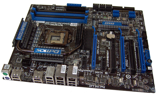
It's pleasing to see MSI sticking with their blue/black theme for the Trinergy. Most of the layout is identical to the GD80/GD-65 motherboards. Notable changes over the lower priced boards from MSI's P55 series are the addition of the NF200 bridge chip and the liberal use of tantalum capacitors (other than the supplied soundcard). Every conventional can type capacitor has been replaced with tantalum types for decoupling, providing lower impedance at high frequencies and also making the board less prone to capacitor related failures long-term.
MSI's confidence in this design is such that they offering an 8 year warranty promotion (non-transferable) on the Trinergy if you pre-order now and register within 30 days. Most enthusiasts will probably be rid of the board well before the warranty expires so they are unlikely to call upon it outside a couple of years. Still, it's good to see this level of confidence (providing MSI does not go the way of the Dodo in the meantime). Normal orders outside MSI's promotion will be subject to a standard 3 year warranty period.
All of the power rails are suitably over-engineered at first approximation, using eight ~30 amp FETs for CPU VCC. Other primary rails like VTT and VDIMM seem to be capable of supplying 50-60 amps peak each - plenty of overclocking overhead. Each of these rails support dynamic power saving which switches off phases to reduce power consumption in light loading conditions. Most overclocking enthusiasts tend to switch off power saving features generally and it appears MSI's engineers do the same thing when you enable OC Genie. The bundled Control Center software also makes some of the power saving menus unavailable when the system is overclocked. We guess this is a good way of ensuring users don't encounter random system crashes when the system is overclocked.
Onboard cooling service is provided by solid screw mounted heatsinks, with the CPU PWM and NF200 sections linked together with a heatpipe. Fin height does not infringe on larger CPU coolers and should allow heatsink mounting in north-south or east-west configurations easily. As always, if overclocking you'll want to keep system temperatures in check and use a fan to cool the heatsink assembly. A small fan pointing at any section of the heatsink should suffice in most situations as the heatpipe seems to transfer heat very well between each portion of the heatsink.
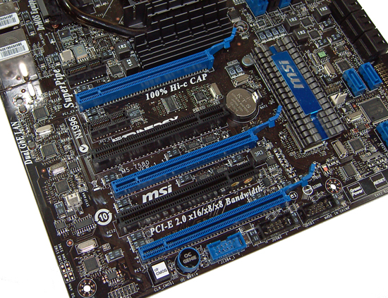
The topmost slot is PCI-E x1 and is configured to accept MSI's bundled soundcard. The blue PCI-E slots placed below are all strung from the NF200 chipset, supporting x16 bandwidth to the first slot in all configurations. If PCI-E slots two and four are populated, both will run at x16 bandwidth unless the third PEG slot is occupied. If all three PEG slots are populated, the PCI-E slots run at x16-x8-x8 bandwidth. Two PCI slots are placed in between the PCI-E slots, and at least one is available for use when all PCI-E slots are occupied. Spacing for the PCI slots in multi-GPU configurations will hinder airflow somewhat.
The lower edge of the board is home to CMOS clear and OC Genie buttons as well as a TPM, one 1394, and two USB headers. Power, reset, and green power buttons are located at the bottom right hand corner of the board using MSI's favored touch sensitive buttons. To the right you'll find the front panel control header block for power, reset buttons, and activity LEDs.
Do note that if the last PCI-E slot is used, access to all buttons and connectors at the lower edge of the board becomes very limited. The power and reset buttons users can work around by using the front panel header to the same effect, but the CMOS Clear button may become inaccessible depending upon the type of GPU cooler employed. MSI would have done well to include a rear panel CMOS-clear button just in case things go awry.
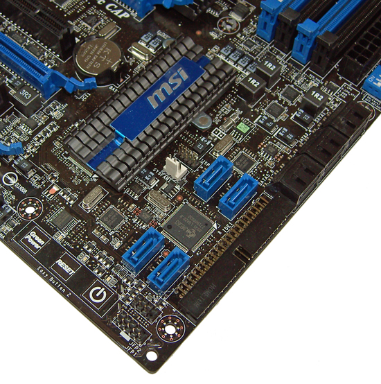
In the lower right hand corner we find an IDE connector, six black right angled SATA ports (Intel P55 PCH), and finally four blue SATA ports (JMicron JMB322) placed in vertical orientation. Unlike the MSI-GD65, the JMicron SATA ports are placed to remain somewhat accessible when GPUs occupy each PCI-E slot.

MSI provides voltage measuring points for all primary rails. A set of leads is included that allows users to plug multimeter leads into the test points for hands free voltage monitoring of each rail. This is the best voltage measurement option we've seen on a board to date. The four DIP switches are 0.1V voltage boost options for CPU VCC and +0.2V for VTT, VDIMM, and PCH rail voltages. The CPU VCC boost is handy in situations where processors are sub-zero cooled and have boot up voltage limits.
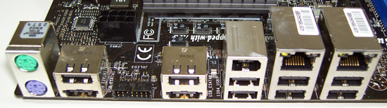
The rear I/O panel connection set is comprised of PS/2 keyboard, PS/2 mouse, OC Dashboard connector, 8 x USB 2.0, 2 x ESATA (USB combo), and 2 x RJ45 LAN ports (Realtek RTL8111DL PCI-E).


12 Comments
View All Comments
Rajinder Gill - Wednesday, December 23, 2009 - link
The conclusion is all on the first page (just read the OVERVIEW/CONCLUSION section), just as it was in the MSI GD-65 and BIOSTAR TPOWER i55 reviews.Rajinder Gill - Wednesday, December 23, 2009 - link
The conclusion is on the first page, just as it was in the MSI GD-65 an BIOSTAR TPOWER i55 reviews.Later