P55 Overclocking Showdown - ASUS, Gigabyte, and EVGA at the OC Corral (Page 6 Updated)
by Rajinder Gill on November 6, 2009 12:00 PM EST- Posted in
- Motherboards
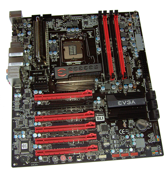
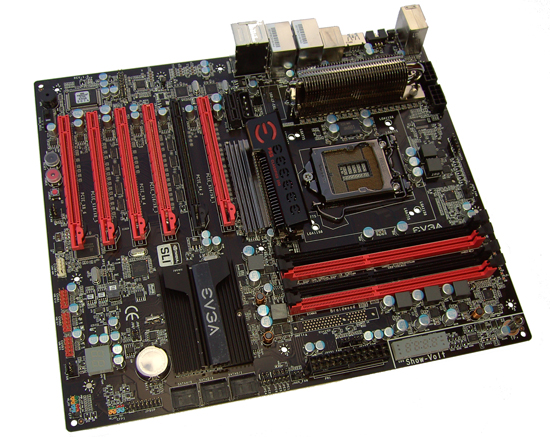
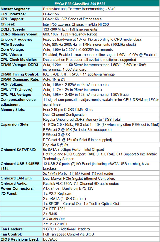
EVGA’s top end offering for P55 is overkill in every single way. Classified specs add a 10-phase Volterra PWM for CPU power, a lower inductance LOTES CPU socket, an onboard digital multi-meter, and an NF200 bridge chip that adds support for triple 16x SLI or CrossFire. Like the P55 FTW E657, version 2 of EVGA’s OCP (overclocking panel) is included giving more than a subtle hint at who this board is designed for.
Priced at $340 or so, this board is more about what EVGA can do than what they should have done for this platform. The existence of X58 fills this segment with a slew of multi-gpu capable boards on the robust and higher performance socket 1366 platform. Nevertheless, we’ve added overclocking results so those who are interested can see how this board fares against others when teamed with the same components and within the same test environment.
Like the E657 model, 7 onboard fan headers are provided with full speed control via BIOS. Due to the addition of the onboard digital multi meter the E659 is classed as E-ATX with dimensions of 304.8mm X 243.8mm (LXW). This might make things a little cramped in smaller PC cases, although we think that anyone choosing a board like this is either going to be someone running an open test bed for benchmarking purposes or is someone who uses a lavish full tower PC case.
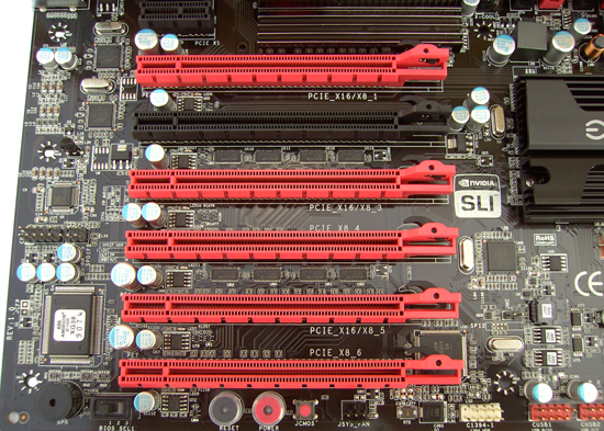
The presence of the NF200 brings a total of six 16x (mechanical) PCI/e slots and one PCI/e x1 slot to the E659. PCI/e X1 at the top, followed by the primary PEG slot running at 16x width in single GPU mode (8x when other PEG slots are occupied).For a full breakdown on lane allocation/link width check the specification table below.
No PCI slots are present on this board, which probably is not a big deal to the intended audience. Slot layout is flexible enough to cater for just about every type of configuration leaving ample upgrade room. We don’t have multi-card performance numbers at this time, although may update later if there is demand to do so.
Underneath the last PCI/e slot, we find power, reset and CMOS clear buttons. A 3 way slider switch is also provided allowing user selection of 3 separate BIOS IC’s. This allows flashing 3 different BIOS files, and also adds a good level of security in the instance of a corrupt BIOS flash. Two USB headers and a IEEE-1394a header are also placed along the bottom edge of the board.
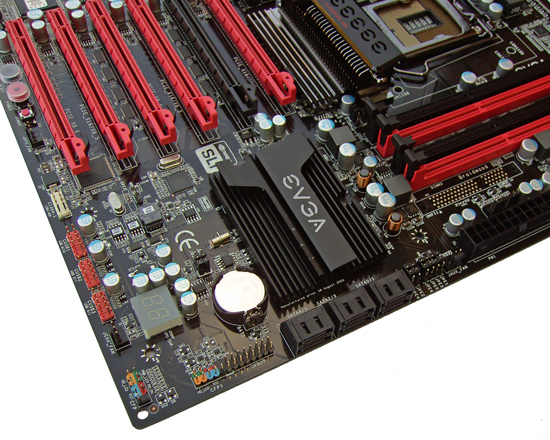
A hex post code display is placed in the lower right corner of the board and over to the left we find 3 BIOS IC’s, one of which is placed within a socket allowing removal if a swap out is required. The CFP1 connector is the EVGA OCP PCB panel connector which allows for on the fly changes 0.1V boost functions to CPU VCore and VTT as well as a post code reader and power, reset and CMOS clear buttons.
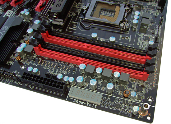
PCI/e disable and X-Cool jumpers are located underneath the DIMM slots. Memory power is supplied by a three phase controller supporting switching speeds up to 640KHz. A test lead is supplied to plug into the positive input socket of the onboard DMM. Test pads for all primary voltage rails are located above the DIMM slots.
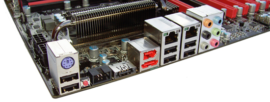
On the rear I/O panel we find 1 x PS2, 7 X USB (1 SATA combo), 1x S/PDIF, 1x Optical, 1 x 1394, 2x RJ45 LAN and 6 audio connectors. A push CMOS reset button is located between the PS2 and S/SPDIF connectors for easy CMOS clear events.
The E657 and E659 models share a practically identical BIOS (refer to screenshots on the E657 page). The only notable changes being the addition of voltage control for the added NF200 on the E659 model, together with an additional compensation adjustment for the CPU.


52 Comments
View All Comments
yyrkoon - Saturday, November 7, 2009 - link
Ok, sorry for the rude comments. But the main reason why this perturbed me, is that something similar happened to a company that I did like a few years back. They lost a lot of revenue because of the situation( and then left the market altogether; yeah . . . guess who ). With that said, I am glad that you guys reported this issue, because at that time, I was seriously considering the board afflicted. Then, I could even go as far back as the terrible capacitors used by many builders, which also caused bad reviews(and feeling from loyal customers)from many reviewers. You would think these companies would learn eventually. Of course, at the time, the builders had no idea these capacitors were going to ruin long term stability ( or maybe they did ? ). Then even in some cases long term was not an issue, because short term stability suffered as well.So, for now on, I suppose I will just have to remember that highly OCable motherboards,are not really dependable for 24/7 operation, and then keep my "mouth" shut :)
I am glad to see one of you does have something from MSI. Now if only the other players would get something out as well.
petergab - Saturday, November 7, 2009 - link
Can you, please, give the socket type of the tested boards? I don't want to start the foxconn/lotes dabate here.And one more clarification: The MSI board (I supoose p55-gd80) was not testes because it had a foxconn socket that burned out OR because the two i7 870 were burned out (on asus)?
Rajinder Gill - Saturday, November 7, 2009 - link
MSI GD80 was not tested because of damage to 2 870 CPU's, one of which was the best sample I had on hand (the one that ran Wprime over 5.2GHz). I've already presented the socket info of the tested boards in the article, but just to recap for you; EVGA boards were on TYCO AMP (E657) and LOTES (E659), ASUS and Gbyte both on Foxconn.MSI's board was ready for review once the CPU damage had already taken place. It was a choice of starting afresh on all 5 boards once again (and risking coming away with even less same CPU comparative info) or running with the almost complete information on 4 boards I had at the time. The latter made more sense to me. Nothing against MSI, their boards were still in beta and undergoing a revision for PCI/e when this all started so they were not in the initial lineup anyway.
later
Raja
petergab - Monday, November 9, 2009 - link
>> Nothing against MSI, their boards were still in beta and undergoing >> a revision for PCI/e when this all started so they were not in the >> initial lineup anyway.Can you explain this in deteils? I think I found something about it 1-2 months ago and haven't saved the address.
Your review was published in Nov. This means you've tested them in Oct, so the planning should have been some time in Sept. As far as I can remember the current MSI board range was on the market before Sept. Does this mean than the MSI has some problems with PCI- PCIE speeds with the current boards? What about the other verndors?
Any links are also appreciated.
Rajinder Gill - Monday, November 9, 2009 - link
Hi,The delay between the article posting and now was simply becasue I tore some fo the content out for the socket burnout stuff a couple of weeks ago. No idea if the MSI PCI/e overclocking patch was post retail or not because I've never had a GD80 in my hands so don't know what to look for per se.
later
Raja
petergab - Monday, November 9, 2009 - link
>> No idea if the MSI PCI/e overclocking patch was post retail or not because...This is exactly what I'm asking about. What was the original problem with this (if any existed)? The fact that you've not considered thier boards talks about some not that trivial issue. What was it? What made you not consider the board?
Rajinder Gill - Monday, November 9, 2009 - link
It's simple;1) At planning stage of who is going to be in the article one, MSI not added to inital lineup because board not ready.
2) By the time revision board is ready, 2 CPU's have been damaged while completing tests of 4 other boards (was in week 4 of testing at this point). Leaving me in a position where all tests must be re-run on every board with a new CPU just to add the MSI board into the report. Given the apparent weakness being experienced and not knowing if I'd be lucky enough even to make it through all 5 boards without another failure I decided to post what I had.
There's nothing more to it. You're reading into this too deeply. If I had anything whatsoever to hide, I would not have posted anything in the first place.
later
Makaveli - Saturday, November 7, 2009 - link
Very happy I just build a P6T Deluxe V2 + 920 D0 combo. Those overclocking numbers look good for the lynnfield setups, but I needed a true and tested platform and with these boards all just coming out I don't trust them.dingetje - Friday, November 6, 2009 - link
wow the p55 platform is totally screwd if this problem persists...any overclocker still oc'ing the hell out of their p55 must be either brave, rich or (michael jackson voice on:) ignoraaaantRaptor88 - Friday, November 6, 2009 - link
Raja:Thank you for you insights..
Can you provide more detail regarding the Max BCLK testing. Were all the boards running AUTO settings? If not, what were their respective settings?
Regards,
Raptor