ATI Radeon HD 4890 vs. NVIDIA GeForce GTX 275
by Anand Lal Shimpi & Derek Wilson on April 2, 2009 12:00 AM EST- Posted in
- GPUs
The Cards and The Test
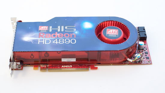
In the AMD department, we received two cards. One was an overclocked part from HIS and the other was a stock clocked part from ASUS. Guess which one AMD sent us for the review. No, it's no problem, we're used to it. This is what happens when we get cards from NVIDIA all the time. They argue and argue for the inclusion of overclocked numbers in GPU reviews when it's their GPU we're looking at. Of course when the tables are turned so are the opinions. We sincerely appreciate ASUS sending us this card and we used it for our tests in this article. The original intent of trying to get a hold of two cards was to run CrossFire numbers, but we only have one GTX 275 and we would prefer to wait until we can compare the two to get into that angle.
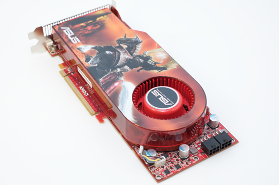
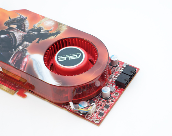
The ASUS card also includes a utility called Voltage Tweaker that allows gamers to increase some voltages on their hardware to help improve overclocking. We didn't have the chance to play with the feature ourselves, but more control is always a nice feature to have.
For the Radeon HD 4890 our hardware specs are pretty simple. Take a 4870 1GB and overclock it. Crank the core up 100 MHz to 850 MHz and the memory clock up 75 MHz to 975 MHz. That's the Radeon HD 4890 in a nutshell. However, to reach these clock levels, AMD revised the core by adding decoupling capacitors, new timing algorithms, and altered the ASIC power distribution for enhanced operation. These slight changes increased the transistor count from 956M to 959M. Otherwise, the core features/specifications (texture units, ROPs, z/stencil) remain the same as the HD4850/HD4870 series.
Most vendors will also be selling overclocked variants that run the core at 900 MHz. AMD would like to treat these overclocked parts like they are a separate entity altogether. But we will continue to treat these parts as enhancements of the stock version whether they come from NVIDIA or AMD. In our eyes, the difference between, say, an XFX GTX 275 and an XFX GTX 275 XXX is XFX's call; the latter is their part enhancing the stock version. We aren't going to look at the XFX 4890 and the XFX 4890 XXX any differently. In doing reviews of vendor's cards, we'll consider overclocked performance closely, but for a GPU launch, we will be focusing on the baseline version of the card.
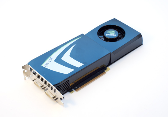
On the NVIDIA side, we received a reference version of the GTX 275. It looks similar to the design of the other GT200 based hardware.
Under the hood here is the same setup as half of a GTX 295 but with higher clock speeds. That means that the GTX 275 has the memory amount and bandwidth of the GTX 260 (448-bit wide bus), but the shader count of the GTX 280 (240 SPs). On top of that, the GTX 275 posts clock speeds closer to the GTX 285 than the GTX 280. Core clock is up 31 MHz from a GTX 280 to 633 MHz, shader clock is up 108 MHz to 1404 MHz, and memory clock is also up 108 MHz to 2322. Which means that in shader limited cases we should see performance closer to the GTX 285 and in bandwicth limited cases we'll still be faster than the GTX 216 because of the clock speed boost across the board.
Rather than just an overclock of a pre-existing card, this is a blending of two configurations combined with an overclock from the two configurations from which it was born. And sure, it's also half a GTX 295, and that is convenient for NVIDIA. It's not just that it's different, it's that this setup should have a lot to offer especially in games that aren't bandwidth limited.
That wraps it up for the cards we're focusing on today. Here's our test system, which is the same as for our GTS 250 article except for the addition of a couple drivers.
The Test
| Test Setup | |
| CPU | Intel Core i7-965 3.2GHz |
| Motherboard | ASUS Rampage II Extreme X58 |
| Video Cards | ATI Radeon HD 4890 ATI Radeon HD 4870 1GB ATI Radeon HD 4870 512MB ATI Radeon HD 4850 NVIDIA GeForce GTX 285 NVIDIA GeForce GTX 280 NVIDIA GeForce GTX 275 NVIDIA GeForce GTX 260 core 216 |
| Video Drivers | Catalyst 8.12 hotfix, 9.4 Beta for HD 4890 ForceWare 185.65 |
| Hard Drive | Intel X25-M 80GB SSD |
| RAM | 6 x 1GB DDR3-1066 7-7-7-20 |
| Operating System | Windows Vista Ultimate 64-bit SP1 |
| PSU | PC Power & Cooling Turbo Cool 1200W |


294 Comments
View All Comments
josh6079 - Thursday, April 2, 2009 - link
I'm one with the opinion that PhysX is good and will only become better in time. Yet, I more than acknowledge the fact that CUDA is going to hinder its adoption so long as nVidia remains unwilling to decouple the two.There was a big thread concerning this on the Video forum, and some people just can't get through the fact that CUDA is proprietary and OpenCL is not. As long as you have that factor, hardware vendors are going to refrain from supporting their competitors proprietary parallel programming and because of that developers will continue to aim for the biggest market segment.
PhysX set the stage for non-CPU physic calculations, but that is no longer going to be an advantageous trait for them. They'll need to improve PhysX itself, and even then they will have to provide it to all consumers -- be it if they have an ATi or nVidia GPU in their system. They'll have to do this because Havok will be doing this with OpenCL to serve as the parallel programming instead of CUDA, thereby allowing Havok GPU-accelerated physics for all OpenCL-compliant GPUs.
tamalero - Sunday, April 5, 2009 - link
the problem is, by the time the PhysX becomes norm, you will be on your NVidia 480GTX :Pit happened to AMD and their X64 technology, took quite a bit to blast off.
haukionkannel - Thursday, April 2, 2009 - link
Well, if these cards reduce the price of earlier cards it's just a good thing :-)From ATI's part changes are not big, but they make the product better. It's better owerclocker than the predessor, it has better power lines. It's just ok upgrade like Phenom 2 was compared to original Phenom (though 4870 was and still is better GPU than Phenom was as an CPU...)
Nvidias 275 offers good upgrade over the 260, so not so bad if those rumors about shady preview samples turns out to be false. If the preview parts really are beefed up versions... Well Nvidia would be in some trouble, and I really think that they would not be that stubid, would'n they? All in all the improvement from 260 to 275 seems to be bigger than 4870 to 4890, so the competition is getting tighter. So far so good.
In real life both producers are keen on developing their DX11 cards to be ready for DX11 launch, so this may be guite boring year in GPU front untill the next generation comes out...
knutjb - Thursday, April 2, 2009 - link
Both cards performed well and the performance differences are small. I can buy the 4890 today on newegg but not the 275. I know the 4890 is a new chip even if it is just a refined RV770 it's still a NEW part. It falls within in an easily understood hierarchy in the 4800 range. Bottom line I know what I'm getting. The 275 I can't buy today and it appears to be another recycled part with unclear origins. Nvidia's track record with musical labeling is bothersome to me. I want to know what I'm buying without having to spend days figuring out which version is the best bang for the buck. Come on Nvidia this is a problem and you can do better than this. The CUDA and PhysX aren't enough to sway me on their own merits since most of the benefits require me to spend more money, yes they add value, but at what expense?.SiliconDoc - Monday, April 6, 2009 - link
nutjob, you're not smart enough to own NVidia. Stick with the card for dummies, the ati.Here's a clue "overclocked 4870 with 1 gig ram not 512, not a 4850 because it has ddr5 not ddr3 - so we call it 4870+ - no wait that would be fair, if we call it 4870 overclocked, uhh... umm.. no we need a better name to make it sound twice as good... let's see 4850, then 4870, so twice as good would be uhh. 4890 ! That's it !
There ya go... So the 4890 is that much better than the 4870, as it is above the 4850, right ? LOL
Maybe they should have called it the 4875, and been HONEST about it like NVidia was > 280 285 ...
No ATI likes to lie, and their dummy fans praise them for it.
Oh well, another red rooster FUD packet blown to pieces.
knutjb - Saturday, April 11, 2009 - link
Dude you missed the whole point, must be the green blurring your vision. Nvidia takes an existing chip and reduces it's capacity or takes one the doesn't meet spec and puts it out as a new product or they take the 8800, then 9800, then the 250, then... that is re-badging. The 4850 and 4830 same same. Grading chip is nothing new but Nvidia keeps rebadging OLD, but good, chips and releases them as if they are NEW which is where my primary complaint about Nvidia gfx cards comes from.4890 might not be an entirely new core but they ADDED to it, rearranged the layout, in the end improving it, they didn't SUBTRACT from it. It is more than a 4870+. It is a very simple concept that apparently you are unable to grasp due to your being such a fanboy. So you don't like ATI, I don't care, I buy whoever has the best bang for the buck that meets my needs not what you think.
ATI looked at the market and decided to hit the midrange and expand down and up from there. They went where most of the money is, in the midrange, not high end gaming. They are hurting and a silly money flag ship doesn't make sense right now. If Nvidia wasn't concerned with the 4890 they wouldn't have released another cut down chip. Put down the pipe and step away from the torch.... Seek help.
SiliconDoc - Thursday, April 23, 2009 - link
So your primary problem is that you think nvidia didn't rework their layout when they changed from G80, to G92, to G92b, and you don't like the fact that they can cover the entire midrange by doing that, because of the NAME they sue when they change the bit width, the shaders, the mem speed etc - BUTWhen aTI does it it's ok because they went for the mid range, you admit the 4850 and 4830 are the same core, but fail to mention the 4870 and fairly include the 4980 as well - because it's OK when ati does it.
Then you ignore all the other winning features of nvidia, and call me names - when I'M THE PERSON TELLING THE TRUTH, AND YOU ARE LYING.
Sorry bubba, doesn't work that way in the real world.
The real horror is ATI doesn't have a core better than the G80/G92/G92b - and the only thing that puts the 4870 and 4890 up to 260/280 levels is the DDR5, which I had to point out to all the little lying spewboys here already.
Now your argument that ATI went for the middle indicates you got that point, and YOU AGREE WITH IT, but just can't bring yourself to say it. Yes, that's the truth as well.
Look at the title of the continuing replies "RE: Another Nvidia knee jerk" - GET A CLUE SON.
lol
Man are you people pathetic. Wow.
Exar3342 - Thursday, April 2, 2009 - link
These are both basically rebadges; deal with it.knutjb - Friday, April 3, 2009 - link
If 3,000,000 more tranistors is "basically a rebadge" you are lost on how much work goes into designing a chip as opposed to changing the stamper on the chip printing machine. I would speculate ATI/AMD has made some interesting progress on their next gen chip design and applied it to the RV770 it worked so they're selling it now to fill a hole in the market.It sounds like you are trying to deal with Nvida's constant rebaging and have to point the finger and claim ATI/AMD is doing it too. Where did the 275 chip come from? Yes it is a good product but how many names do you want it called?
I have bought just as many Nvidia cards as I have ATI/AMD based on bang for the buck, just calling it like I see it...
SiliconDoc - Monday, April 6, 2009 - link
Well, they worked it for overclocking - and apparently did a fine job of that - but it is a rebadging, none the less.It seems the less than one half of one percent "new core" transistors are used as a sort of multi capacitor ring around the outside of the core, for overclocking legs. Not bad, but not a new core. I do wonder as they hinted they "did some rearranging" - if they had to waste some of those on the core works - lengthening or widening or bridging this or that - or connections to the bois for volt modding or what have you.
When eother company moves to a smaller die, a similar effect is had for the cores, some movements and fittings and optimizations always occur, although this site always jumped on the hate and lie bandwagon to screech about "rebranding" - as well as "confusing names" since the cards were not all the same... bit width, memory type, size, shaders, etc.
So I'm sure we would hear about the IMMENSE VERSATILITY of the awesome technology of the ati core (if they did the same thing with their core).
However, they've done a rebranding a ring around the overclock. Nice, but same deal.
Can you tell us how much more epxensive it's going to be to produce since derak and anand decided to "not mention the cost" since they didn't have the green monster to bash about it ?
Oh that's right, it's RUDE to mention the extra cost when the red rooster company is burning through a billion a year they don't have - ahh, the great sales numbers, huh ?