ATI Radeon HD 4890 vs. NVIDIA GeForce GTX 275
by Anand Lal Shimpi & Derek Wilson on April 2, 2009 12:00 AM EST- Posted in
- GPUs
The Cards and The Test
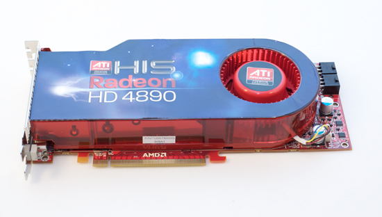
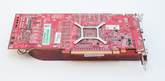
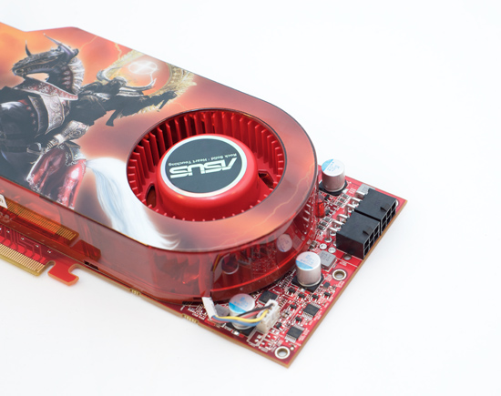
In the AMD department, we received two cards. One was an overclocked part from HIS and the other was a stock clocked part from ASUS. Guess which one AMD sent us for the review. No, it's no problem, we're used to it. This is what happens when we get cards from NVIDIA all the time. They argue and argue for the inclusion of overclocked numbers in GPU reviews when it's their GPU we're looking at. Of course when the tables are turned so are the opinions. We sincerely appreciate ASUS sending us this card and we used it for our tests in this article. The original intent of trying to get a hold of two cards was to run CrossFire numbers, but we only have one GTX 275 and we would prefer to wait until we can compare the two to get into that angle.
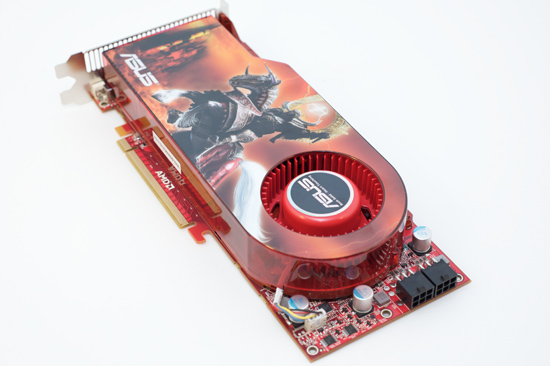
The ASUS card also includes a utility called Voltage Tweaker that allows gamers to increase some voltages on their hardware to help improve overclocking. We didn't have the chance to play with the feature ourselves, but more control is always a nice feature to have.
For the Radeon HD 4890 our hardware specs are pretty simple. Take a 4870 1GB and overclock it. Crank the core up 100 MHz to 850 MHz and the memory clock up 75 MHz to 975 MHz. That's the Radeon HD 4890 in a nutshell. However, to reach these clock levels, AMD revised the core by adding decoupling capacitors, new timing algorithms, and altered the ASIC power distribution for enhanced operation. These slight changes increased the transistor count from 956M to 959M. Otherwise, the core features/specifications (texture units, ROPs, z/stencil) remain the same as the HD4850/HD4870 series.
Most vendors will also be selling overclocked variants that run the core at 900 MHz. AMD would like to treat these overclocked parts like they are a separate entity altogether. But we will continue to treat these parts as enhancements of the stock version whether they come from NVIDIA or AMD. In our eyes, the difference between, say, an XFX GTX 275 and an XFX GTX 275 XXX is XFX's call; the latter is their part enhancing the stock version. We aren't going to look at the XFX 4890 and the XFX 4890 XXX any differently. In doing reviews of vendor's cards, we'll consider overclocked performance closely, but for a GPU launch, we will be focusing on the baseline version of the card.
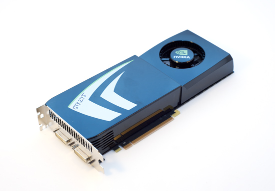
On the NVIDIA side, we received a reference version of the GTX 275. It looks similar to the design of the other GT200 based hardware.
Under the hood here is the same setup as half of a GTX 295 but with higher clock speeds. That means that the GTX 275 has the memory amount and bandwidth of the GTX 260 (448-bit wide bus), but the shader count of the GTX 280 (240 SPs). On top of that, the GTX 275 posts clock speeds closer to the GTX 285 than the GTX 280. Core clock is up 31 MHz from a GTX 280 to 633 MHz, shader clock is up 108 MHz to 1404 MHz, and memory clock is also up 108 MHz to 2322. Which means that in shader limited cases we should see performance closer to the GTX 285 and in bandwicth limited cases we'll still be faster than the GTX 216 because of the clock speed boost across the board.
Rather than just an overclock of a pre-existing card, this is a blending of two configurations combined with an overclock from the two configurations from which it was born. And sure, it's also half a GTX 295, and that is convenient for NVIDIA. It's not just that it's different, it's that this setup should have a lot to offer especially in games that aren't bandwidth limited.
That wraps it up for the cards we're focusing on today. Here's our test system, which is the same as for our GTS 250 article except for the addition of a couple drivers.
The Test
| Test Setup | |
| CPU | Intel Core i7-965 3.2GHz |
| Motherboard | ASUS Rampage II Extreme X58 |
| Video Cards | ATI Radeon HD 4890 ATI Radeon HD 4870 1GB ATI Radeon HD 4870 512MB ATI Radeon HD 4850 NVIDIA GeForce GTX 285 NVIDIA GeForce GTX 280 NVIDIA GeForce GTX 275 NVIDIA GeForce GTX 260 core 216 |
| Video Drivers | Catalyst 8.12 hotfix, 9.4 Beta for HD 4890 ForceWare 185.65 |
| Hard Drive | Intel X25-M 80GB SSD |
| RAM | 6 x 1GB DDR3-1066 7-7-7-20 |
| Operating System | Windows Vista Ultimate 64-bit SP1 |
| PSU | PC Power & Cooling Turbo Cool 1200W |


294 Comments
View All Comments
SiliconDoc - Monday, April 6, 2009 - link
Don't worry, it is mentioned in the article their overclocking didn't have good results, so they're keying up a big fat red party for you soon.They wouldn't dare waste the opportunity to crow and strut around.
This was about announcing the red card, slamming nvidia for late to market, and denouncing cuda and physx, and making an embarrassingly numberous amount of "corrections" to the article, including declaring the 2560 win, not a win anymore, since the red card didn't do it.
That's ok, be ready for the change back to 2560 is THE BESt and wins, when the overclock review comes out.
:)
Don't worry be happy.
tamalero - Thursday, April 9, 2009 - link
SD, you seriously have a mental problem right?I noticed that you keep bashing, being sarcastically insultive (betwen other things.) to anyone who supports ati.
SiliconDoc - Thursday, April 23, 2009 - link
No, not true at all, there are quite a few posts where the person declaring their ATI fealty doesn't lie their buttinski off - and those posts I don't counter.Sorry, you must be a raging goofball too who can't spot liars.
It's called LOGIC, that's what you use against the lairs - you know, scientific accuracy.
Better luck next time - If you call me wrong I'll post a half dozen red rooster rooters in this thread that don't lie in what they say and you'll see I didn't respond.
Now, you can apologize any time, and I'll give you another chance, since you were wrong this time.
Nfarce - Thursday, April 2, 2009 - link
I just finished a mid-range C2D build, and decided to go with the HD 4870 512MB version for $164.99 (ASUS, no sale at NE, but back up to $190 now). This was my first ATI card and it was a no-brainer. While the 4890 is a better card, to me, it is not worth the nearly $100 more, especially considering I'm gaming at either 1920x1200 on a 40" LCD TV or a 22" LCD monitor at 1680x1050.Nvidia has lost me after 12 years as a fanboy for the time being, I suppose. What I will do here when I have more time is determine if buying another 4870 512MB for CrossFire will be the better bang for my resolutions or eventually moving up to the 4890 when the price drops this summer and then sell the 4870.
Thanks for the GREAT review AT, and now I have my homework cut out for me for comparisons with your earlier GPU reviews.
Jamahl - Thursday, April 2, 2009 - link
Good job with tidying up the conclusion Anand.Russ2650 - Thursday, April 2, 2009 - link
I've read that the 4890 has 959M transistors, 3M more than the 4870.Gary Key - Thursday, April 2, 2009 - link
That is correct and is discussed on page 3. The increase in die size is due to power delivery improvements to handle the increased clock speeds.Warren21 - Thursday, April 2, 2009 - link
Maybe the tables should be updated to reflect this?Gary Key - Thursday, April 2, 2009 - link
They are... :)helpmespock - Thursday, April 2, 2009 - link
I've been sitting on my 8800GT for a while now and was thinking about going to a 4870 1GB model, but now I may hold off and see what prices do.If the 4890/275 force the 4870 down in price then great I'll go with that, but on the other hand if prices slip from the new parts off of the $250 mark then I'll be tempted by that instead.
Either way I think I'm waiting to see how the market shakes out and in the end I, the consumer, will win.