The Radeon HD 4850 & 4870: AMD Wins at $199 and $299
by Anand Lal Shimpi & Derek Wilson on June 25, 2008 12:00 AM EST- Posted in
- GPUs
Wrapping Up the Architecture and Efficiency Discussion
Engineering is all about tradeoffs and balance. The choice to increase capability in one area may decrease capability in another. The addition of a feature may not be worth the cost of including it. In the worst case, as Intel found with NetBurst, an architecture may inherently flawed and a starting over down an entirely different path might be the best solution.
We are at a point where there are quite a number of similarities between NVIDIA and AMD hardware. They both require maintaining a huge number of threads in flight to hide memory and instruction latency. They both manage threads in large blocks of threads that share context. Caching, coalescing memory reads and writes, and handling resource allocation need to be carefully managed in order to keep the execution units fed. Both GT200 and RV770 execute branches via dynamic predication of direction a thread does not branch (meaning if a thread in a warp or wavefront branches differently from others, all threads in that group must execute both code paths). Both share instruction and constant caches across hardware that is SIMD in nature servicing multiple threads in one context in order to effect hardware that fits the SPMD (single program multiple data) programming model.
But the hearts of GT200 and RV770, the SPA (Steaming Processor Array) and the DPP (Data Parallel Processing) Array, respectively, are quite different. The explicitly scalar one operation per thread at a time approach that NVIDIA has taken is quite different from the 5 wide VLIW approach AMD has packed into their architecture. Both of them are SIMD in nature, but NVIDIA is more like S(operation)MD and AMD is S(VLIW)MD.
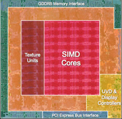
AMD's RV770, all built up and pretty
Filling the execution units of each to capacity is a challenge but looks to be more consistent on NVIDIA hardware, while in the cases where AMD hardware is used effectively (like Bioshock) we see that RV770 surpasses GTX 280 in not only performance but power efficiency as well. Area efficiency is completely owned by AMD, which means that their cost for performance delivered is lower than NVIDIA's (in terms of manufacturing -- R&D is a whole other story) since smaller ICs mean cheaper to produce parts.
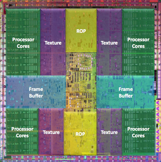
NVIDIA's GT200, in all its daunting glory
While shader/kernel length isn't as important on GT200 (except that the ratio of FP and especially multiply-add operations to other code needs to be high to extract high levels of performance), longer programs are easier for AMD's compiler to extract ILP from. Both RV770 and GT200 must balance thread issue with resource usage, but RV770 can leverage higher performance in situations where ILP can be extracted from shader/kernel code which could also help in situations where the GT200 would not be able to hide latency well.
We believe based on information found on the CUDA forums and from some of our readers that G80's SPs have about a 22 stage pipeline and that GT200 is also likely deeply piped, and while AMD has told us that their pipeline is significantly shorter than this they wouldn't tell us how long it actually is. Regardless, a shorter pipeline and the ability to execute one wavefront over multiple scheduling cycles means massive amounts of TLP isn't needed just to cover instruction latency. Yes massive amounts of TLP are needed to cover memory latency, but shader programs with lots of internal compute can also help to do this on RV770.
All of this adds up to the fact that, despite the advent of DX10 and the fact that both of these architectures are very good at executing large numbers of independent threads very quickly, getting the most out of GT200 and RV770 requires vastly different approaches in some cases. Long shaders can benefit RV770 due to increased ILP that can be extracted, while the increased resource use of long shaders may mean less threads can be issued on GT200 causing lowered performance. Of course going the other direction would have the opposite effect. Caches and resource availability/management are different, meaning that tradeoffs and choices must be made in when and how data is fetched and used. Fixed function resources are different and optimization of the usage of things like texture filters and the impact of the different setup engines can have a large (and differing with architecture) impact on performance.
We still haven't gotten to the point where we can write simple shader code that just does what we want it to do and expect it to perform perfectly everywhere. Right now it seems like typical usage models favor GT200, while relative performance can vary wildly on RV770 depending on how well the code fits the hardware. G80 (and thus NVIDIA's architecture) did have a lead in the industry for months before R600 hit the scene, and it wasn't until RV670 that AMD had a real competitor in the market place. This could be part of the reason we are seeing fewer titles benefiting from the massive amount of compute available on AMD hardware. But with this launch, AMD has solidified their place in the market (as we will see the 4800 series offers a lot of value), and it will be very interesting to see what happens going forward.


215 Comments
View All Comments
BusterGoode - Sunday, June 29, 2008 - link
Thanks, great article by the way Anandtech is my first stop for reviews.jay401 - Wednesday, June 25, 2008 - link
Good but I just wish AMD would give it a full 512-bit memory bus bandwidth. Tired of 256-bit. It's so dated and it shows in the overall bandwidth compared to NVidia's cards with 512-bit bus widths. All that fancy GDDR4/5 and it doesn't actually shoot them way ahead of NVidia's cards in memory bandwidth because they halve the bus width by going with 256-bit instead of 512-bit. When they offer 512-bit the cards will REALLY shine.Spoelie - Thursday, June 26, 2008 - link
Except that when R600 had a 512bit bus, it didn't show any advantage over RV670 with a 256bit bus. And that was with GDDR3 vs GDDR3, not GDDR5 like in RV770 case.JarredWalton - Thursday, June 26, 2008 - link
R600 was 512-bit ring bus with 256-bit memory interface (four 64-bit interfaces). http://www.anandtech.com/showdoc.aspx?i=2552&p...">Read about it here for a refresh. Besides being more costly to implement, it used a lot of power and didn't actually end up providing provably better performance. I think it was an interesting approach that turned out to be less than perfect... just like NetBurst was an interesting design that turned out to have serious power limitations.Spoelie - Thursday, June 26, 2008 - link
Except that it was not, that was R520 ;) and R580 is the X19x0 series. That second one proved to be the superior solution over time.R600 is the x2900xt, and it had a 1024bit ring bus with 512bit memory interface.
DerekWilson - Sunday, June 29, 2008 - link
yeah, r600 was 512-bithttp://www.anandtech.com/showdoc.aspx?i=2988&p...">http://www.anandtech.com/showdoc.aspx?i=2988&p...
looking at external bus width is an interesting challenge ... and gddr5 makes things a little more crazy in that clock speed and bus width can be so low with such high data rates ...
but the 4870 does have 16 memory modules on it ... so that's a bit of a barrier to higher bit width busses ...
JarredWalton - Wednesday, June 25, 2008 - link
I'd argue that the 512-bit memory interface on NVIDIA's cards is at least partly to blame for their high pricing. All things being equal, a 512-bit interface costs a lot more to implement than a 256-bit interface. GDDR5 at 900MHz is effectively the same as GDDR3 at 1800MHz... except no one is able to make 1800MHz GDDR3. Latencies might favor one or the other solution, but latencies are usually covered by caching and other design decisions in the GPU world.geok1ng - Wednesday, June 25, 2008 - link
The tests showed what i feared: my 8800GT is getting old to pump my Apple at 2560x1600 even without AA! But the tests also showed that the 512MB of DDR5 on the 4870 justifies the higher price tag over the 4850, something that the 3870/3850 pair failed to demonstrate. It remains the question: will 1GB of DDR5 detrone NVIDIA and rule the 30 inches realm of single GPU solutions?IKeelU - Wednesday, June 25, 2008 - link
"It is as if AMD and NVIDIA just started pulling out hardware and throwing it at eachother"This makes me crack up...I just imagine two bruised and sweaty middle-aged CEO's flinging PCBs at each other, like children in a snowball fight.
Thorsson - Wednesday, June 25, 2008 - link
The heat is worrying. I'd like to see how aftermarket coolers work with a 4870.