The Radeon HD 4850 & 4870: AMD Wins at $199 and $299
by Anand Lal Shimpi & Derek Wilson on June 25, 2008 12:00 AM EST- Posted in
- GPUs
That Darn Compute:Texture Ratio
With its GT200 GPU, NVIDIA increased compute resources by nearly 90% but only increased texture processing by 25%, highlighting a continued trend in making GPUs even more powerful computationally. Here's another glance at the GT200's texture address and filter units:
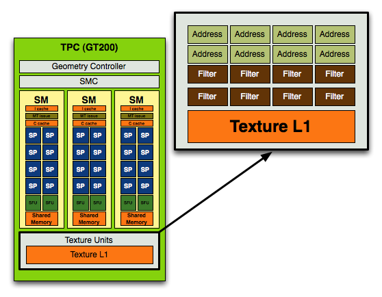
Each TPC, of which there are 10, has eight address and eight filter units. Now let's look at RV770:
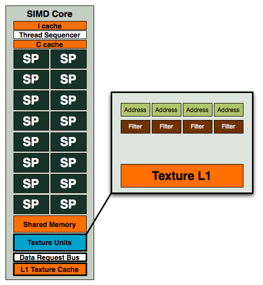
Four address and four filter units, while AMD maintains the same 1:1 address-to-filter ratio that NVIDIA does, the ratio of compute-to-texture in RV770 is significantly higher.
| AMD RV770 | AMD RV670 | NVIDIA GT200 | NVIDIA G92 | |
| # of SPs | 160 | 64 | 240 | 128 |
| Texture Address/Filter Units | 40 / 40 | 16 / 16 | 80 / 80 | 64 / 64 |
| Compute to Texture Ratio | 4:1 | 4:1 | 3:1 | 2:1 |
The table above illustrates NVIDIA's trend of increasing the compute to texture ratio from 2:1 in G92 to 3:1 in GT200. AMD arguably overshot with RV670 and its 4:1 ratio and thus didn't need to adjust it with RV770. Even while staying still at 4:1 with RV770, AMD's ratio is still more aggressively geared towards compute than NVIDIA's is. That does mean that more texture bound games will do better on NVIDIA hardware (at least proportionally), while more compute intensive games may do better on RV770.
AMD did also make some enhancements to their texture units as well. By doing some "stuff" that they won't tell us about, they improved the performance per mm^2 by 70%. Texture cache bandwidth has also been doubled to 480 GB/s while bandwidth between each L1 cache and L2 memory is 384 GB/s. L2 caches are aligned with memory channels of which there are four interleaved channels (resulting in 8 L2 caches).
Now that texture units are linked to both specific SIMD cores and individual L1 texture caches, we have an increase in total texturing ability due to the increase in SIMD cores with RV770. This gives us a 2.5x increase in the number of 8-bit per component textures we can fetch and bilinearly filter per clock, but only a 1.25x increase in the number of fp16 textures (as fp16 runs at half rate and fp32 runs at one quarter rate). It was our understanding that fp16 textures could run at full speed on R600, so the 1.25x increase in performance for half rate texturing of fp16 data makes sense.
Even though fp32 runs at quarter rate, with the types of texture fetches we would need to do, AMD says that we could end up being external memory bandwidth bound before we are texture filtering hardware bound. If this is the case, then the design decision to decrease rates for higher bit-depth textures makes sense.
| AMD RV770 | AMD RV670 | |
| L1 Texture Cache | 10 x 16KB (160KB total) | 32KB |
| L2 Texture Cache | I can has cache size? | 256KB |
| Vertex Cache | ? | 32KB |
| Local Data Share | 16KB | None |
| Global Data Share | 16KB | ? |
Even though AMD wouldn't tell us L1 cache sizes, we had enough info left over from the R600 time frame to combine with some hints and extract the data. We have determined that RV770 has 10 distinct 16k caches. This is as opposed to the single shared 32k L1 cache on R600 and gives us a total of 160k of L1 cache. We know R600's L2 cache was 256k, and AMD told us RV770 has a larger L2 cache, but they wouldn't give us any hints to help out.


215 Comments
View All Comments
BusterGoode - Sunday, June 29, 2008 - link
Thanks, great article by the way Anandtech is my first stop for reviews.jay401 - Wednesday, June 25, 2008 - link
Good but I just wish AMD would give it a full 512-bit memory bus bandwidth. Tired of 256-bit. It's so dated and it shows in the overall bandwidth compared to NVidia's cards with 512-bit bus widths. All that fancy GDDR4/5 and it doesn't actually shoot them way ahead of NVidia's cards in memory bandwidth because they halve the bus width by going with 256-bit instead of 512-bit. When they offer 512-bit the cards will REALLY shine.Spoelie - Thursday, June 26, 2008 - link
Except that when R600 had a 512bit bus, it didn't show any advantage over RV670 with a 256bit bus. And that was with GDDR3 vs GDDR3, not GDDR5 like in RV770 case.JarredWalton - Thursday, June 26, 2008 - link
R600 was 512-bit ring bus with 256-bit memory interface (four 64-bit interfaces). http://www.anandtech.com/showdoc.aspx?i=2552&p...">Read about it here for a refresh. Besides being more costly to implement, it used a lot of power and didn't actually end up providing provably better performance. I think it was an interesting approach that turned out to be less than perfect... just like NetBurst was an interesting design that turned out to have serious power limitations.Spoelie - Thursday, June 26, 2008 - link
Except that it was not, that was R520 ;) and R580 is the X19x0 series. That second one proved to be the superior solution over time.R600 is the x2900xt, and it had a 1024bit ring bus with 512bit memory interface.
DerekWilson - Sunday, June 29, 2008 - link
yeah, r600 was 512-bithttp://www.anandtech.com/showdoc.aspx?i=2988&p...">http://www.anandtech.com/showdoc.aspx?i=2988&p...
looking at external bus width is an interesting challenge ... and gddr5 makes things a little more crazy in that clock speed and bus width can be so low with such high data rates ...
but the 4870 does have 16 memory modules on it ... so that's a bit of a barrier to higher bit width busses ...
JarredWalton - Wednesday, June 25, 2008 - link
I'd argue that the 512-bit memory interface on NVIDIA's cards is at least partly to blame for their high pricing. All things being equal, a 512-bit interface costs a lot more to implement than a 256-bit interface. GDDR5 at 900MHz is effectively the same as GDDR3 at 1800MHz... except no one is able to make 1800MHz GDDR3. Latencies might favor one or the other solution, but latencies are usually covered by caching and other design decisions in the GPU world.geok1ng - Wednesday, June 25, 2008 - link
The tests showed what i feared: my 8800GT is getting old to pump my Apple at 2560x1600 even without AA! But the tests also showed that the 512MB of DDR5 on the 4870 justifies the higher price tag over the 4850, something that the 3870/3850 pair failed to demonstrate. It remains the question: will 1GB of DDR5 detrone NVIDIA and rule the 30 inches realm of single GPU solutions?IKeelU - Wednesday, June 25, 2008 - link
"It is as if AMD and NVIDIA just started pulling out hardware and throwing it at eachother"This makes me crack up...I just imagine two bruised and sweaty middle-aged CEO's flinging PCBs at each other, like children in a snowball fight.
Thorsson - Wednesday, June 25, 2008 - link
The heat is worrying. I'd like to see how aftermarket coolers work with a 4870.