ASUS P5E3 Premium: One to Rule them All…
by Kris Boughton on February 20, 2008 12:15 AM EST- Posted in
- Motherboards
Memory Overclocking
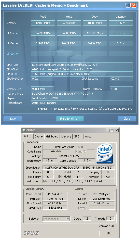
These are some of the highest memory read scores and lowest latencies we have ever seen on an Intel chipset. This is exactly where DDR3 starts to show its real power.
It's hard to argue with the performance potential this system brings at these settings, something that current X38 users might find impossible when aiming for total stability. Perhaps the most impressive point in this accomplishment is that our MCH required only 1.35V in order to run hour after hour of Prime95 or other stress tests without error. There are those that may believe this is not much to speak of, but the combination of high CPU speed and low tRD is brutal on the MCH - something we plan to explore soon in great detail. In fact, this is exactly where the X48 chipset begins to shine - in some of the situations where the X38 would either fall flat on its face or require voltages well in excess of those we feel comfortable using on a daily basis.
CPU Overclocking
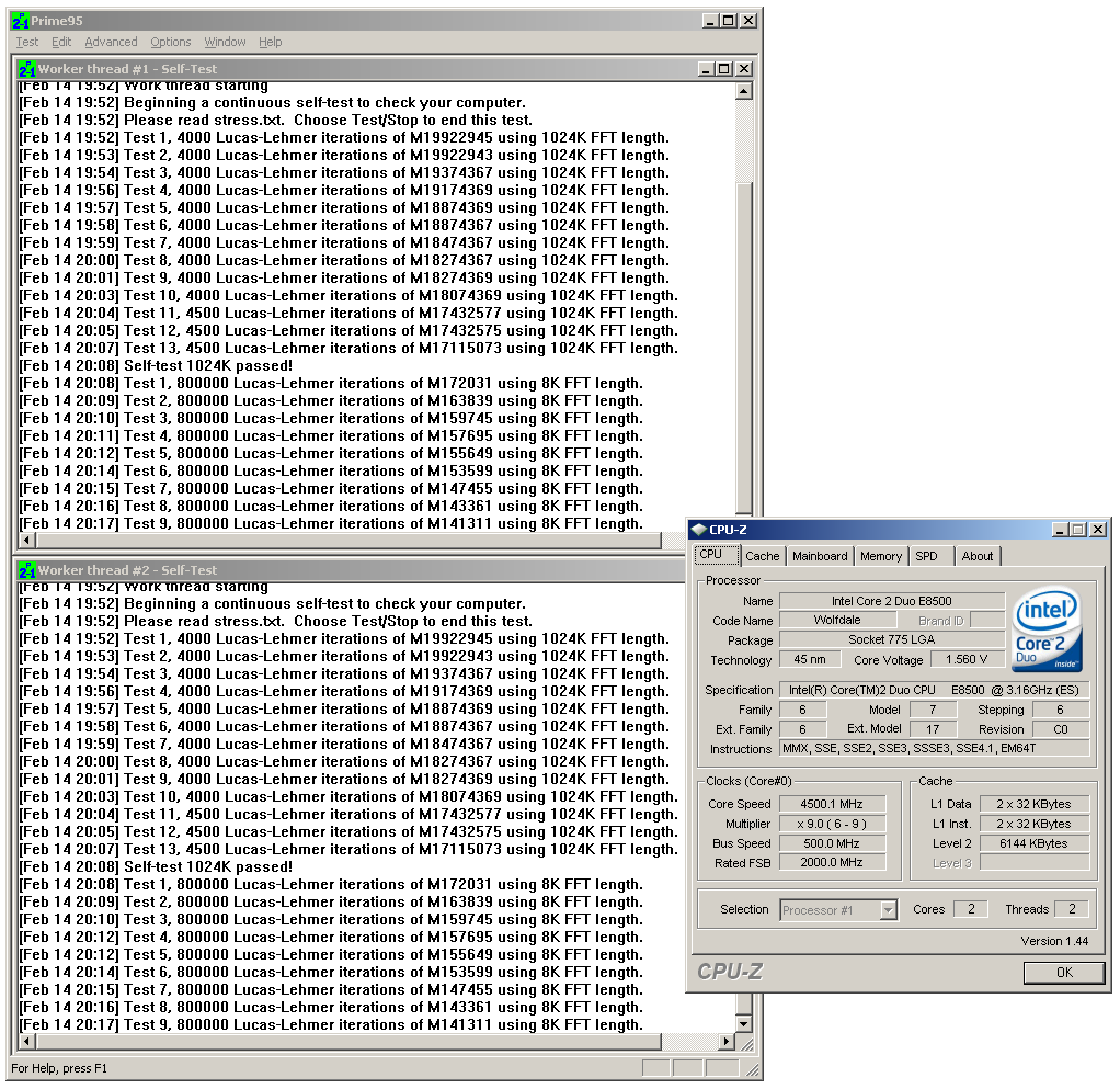 While 4.5GHz on a 45nm dual-core might not seem that impressive, we were able to get this system stable at these settings with water-cooling alone. Click to view Prime95 in action. |
The typical 45nm dual-core usually tops out around 4.0 to 4.2GHz on water-cooling or air-cooling alone, at least when it comes to achieving a truly stable overclock. Getting our E8500 sample to 4.5GHz stable took a little patience and a lot more Vcore than we feel comfortable using. Nevertheless, we ran Prime95 here for days while keeping temperatures under control (about 55C maximum in a 20C room). Most people who overclock knows just how difficult this can be.
Again, we must give a lot of credit in the success of this overclock to the power of the X48 chipset. This is also a great demonstration of ASUS' ability to design a very capable VRM circuit. Current draw under full-load at these speeds is impressive to say the least. Any other less capable power delivery design probably would have gone down in a blaze of glory (we had several in the labs that did just that trying to keep up with this board). This all just goes to show that although not specifically built for gaming per say, the P5E3 Premium is more than capable of keeping up with ASUS' very own R.O.G. line of motherboards. (Ed: Now if we could just do something about the lack of SLI….)
FSB Wars: Return of the Stupid-High Screenshot
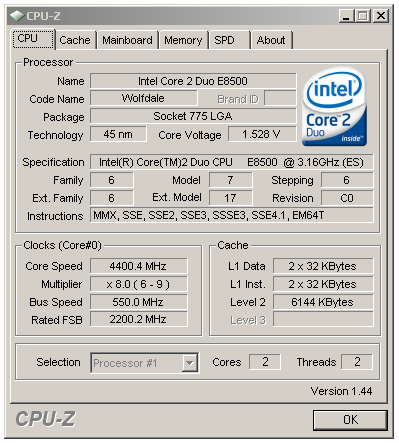
For the general bemusement of the FSB crowd, we decided to include a screenshot of our board's maximum FSB using stock cooling and respectable voltages. While higher FSB speeds may be achievable, we can hardly imaging using them at this point. Intel's 45nm dual-core speed binning process promises to play a much more active role in the release of all future CPUs. Those that think they are going to pay for a budget chip and then turn around and overclock it to the same speeds as top-end Extreme CPUs are in for a rude awakening based on our early retail results. Keep in mind that our absolute maximum stable overclock was barely made using a multiplier less than the E8500's stock 9.5x value and you should begin to see one reason why these uber-high FSB speeds are just plain unneeded.
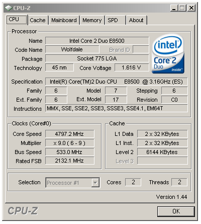
No quick look at overclocking performance would be complete without the obligatory maximum CPU frequency suicide-run screenshot. Just what the maximum achievable frequency was had more to do with our nerves than anything else. Given the voltage, our E8500 was more than happy to continue scaling ever higher. At some point though we said enough is enough and called it quits - that point came when we saw that we were subjecting our poor 45nm CPU to over 1.6V, simply a voltage that will require your credit card to be handy for another CPU in short time. Quite simply, we believe any voltage over 1.45V is asking for danger on the 45nm processors and conversations with Intel seem to back-up our beliefs right now. Our only solace is that we were quick when it came to gathering these results.


32 Comments
View All Comments
AllanLim - Wednesday, February 20, 2008 - link
My bad...missed those.AllanLim - Wednesday, February 20, 2008 - link
But I still maintain my position until retail samples show up...squito - Wednesday, February 20, 2008 - link
I can still taste the RDRAM and i820 motherboards ...Orbs - Wednesday, February 20, 2008 - link
The introduction to the article aludes to the fact that in the not-too-distant future, we may have to choose platforms at the expense of component choices such as graphics cards.I think that's already the case and has been for some time. If I want an Intel-based mobo, say goodbye to SLI. If I want SLI, I have to choose nVidia's chipset.
Unless Intel's next platform makes it impossible to choose any graphics card (not multi-card solution, but single-card) then it's no worse than what we have today.
That said, I think we would all welcome the ability to run any two (or three) add-in cards in SLI or CrossFire for graphics and/or physics on any motherboard. That would make it much easier to decide which components to buy as we could judge them on their individual merits and not on what limitations they impose on the rest of the system.
Cykoth - Wednesday, February 20, 2008 - link
You know? This is all well and good....but Anandtech has never completed the review of the Asus Striker II Formula. Based upon the quick blog put out by them, and the feature set, I purchased one for my new build. I had NOTHING but trouble out of it. Even after BIOS updates, extra case fans, and finally an 18Inch fan stuck in the side of the case, it still wouldn't run stabily. I even had problems with the LAN adapters accepting dynamic IP's and therefore no gateway to the internet. Then, no response from ASUS tech support at all. I used to be a HUGE Asus fan....but I've RMA'ed that piece O' crap, and am waiting on my P35 chipset Gigabyte so I can have a system that doesn't REQUIRE water cooling to function.Really Anandtech.....will you EVER complete the Striker II Formula review? I'm interested to know how you got it to work.
Cyko
tmarques - Wednesday, February 20, 2008 - link
The winbond chip is the SuperIO or hardware monitoring chip.The BIOS chip in ASUS new motherboards is, usually, a flash SPI chip, that sits next to the SPI debug connector.
The P5E3 Premium SPI BIOS chip and connector are next to the CMOS battery.
kjboughton - Wednesday, February 20, 2008 - link
Yep, you're absolutely right. Confused the chip with something else. Thank you.RobinBee - Wednesday, February 20, 2008 - link
I see these logos on AnandTech's pictures.These (ASUS) logos must be removed, before using a motherboard.
Does AnandTech test MBs without removing those logos?
If so, a MB's passive cooling is not optimal.
Rajinder Gill - Wednesday, February 20, 2008 - link
The 'Ai Lifestyle' logo is glued onto the Southbridge heatsink block. Even if removed, there are no fins to take advantage of the airflow, other than the slightly reduced thermal resistance - no real gains in removal there.The blue Asus logo plate has a heatpipe passing thru it, via a hole on the left of the Nortbridge heatsink. Meaning one would have to break or cut it, to take it off the heatsink. Obviously, there would be some benefit to removal, but perhaps the benefits of an active warranty are better than 2-3 degrees of temp drop..
We tend only to remove things that are removable by design, in this case neither of those logo plates are designed to be removed.. Hence we have no issue chagning out thermal paste if we deem it necessary.
regards
supremelaw - Wednesday, February 20, 2008 - link
Forgive me if this question reveals my ignoranceon this one point: I obviously need answers,
and still don't have answers ...
As someone who is responsible for keeping several
backup copies of a database up-to-date, I have
found that x4 PCI-Express lanes cause a lower
ceiling on the performance of RAID 0 storage
than x8 PCI-Express lanes in any given expansion
slot.
One of the reasons why we purchased the ASUS
P5W64 WS Professional, is the use of 4 x x16 slots
which can be assigned 8-8-4-8 PCI-Express lanes
(one option mentioned in the User Manual).
The better RAID controllers that we are considering
all require x8 PCI-Express lanes, instead of x4 lanes,
e.g. Areca, Highpoint, etc.
Someone is now going to recommend here that
we forego SLI or Crossfire and use one of the
x16 video slots for the RAID controller.
OK: I don't mind going without dual video cards,
because I don't need to live and work on the
bleeding edge of graphics technology.
BUT ... here's the rub: if you contact Tech Support
at the companies that manufacture RAID controllers,
they are typically unable to confirm if their x8 lane
controllers will work in x16 video slots.
"Try it and tell us what happens," they all say!
If that combination does NOT work, the RAID controller
must be inserted in the only remaining x16 slot,
which only gets x4 PCI-Express lanes, NOT x8!
That combination just proves that such motherboards
were the WRONG CHOICE from day one.
I thought that PCI-Express was designed to provide
greater speed for most peripheral subsystems,
NOT JUST graphics cards.
WHAT GIVES?
Sincerely yours,
/s/ Paul Andrew Mitchell
Webmaster, Supreme Law Library
http://www.supremelaw.org/">http://www.supremelaw.org/