ASUS ROG Rampage Formula: Why we were wrong about the Intel X48
by Kris Boughton on January 25, 2008 4:30 AM EST- Posted in
- Motherboards
The Rules of Working with tRD: What's Allowed and What Isn't
We mentioned earlier that there are a few rules pertaining to the modification of the default tRD value for a particular memory subsystem configuration. These rules are actually more of a set of equations that we have derived in order to assist the user in pre-determining whether or not a system will POST and operate given the settings in question. They can also be used to explain after the fact why certain configurations refuse to function.
In actuality, there is only one requirement that must be satisfied when setting tRD: The MCH must have a minimum amount of time to complete the clock crossing procedure for each data bit translated from one clocking domain to the other. We have shown the equation below for those that care to know. Unfortunately it does not lend itself well to being solved as the input variables ("t0" and "tckxss") are not readily obtainable.
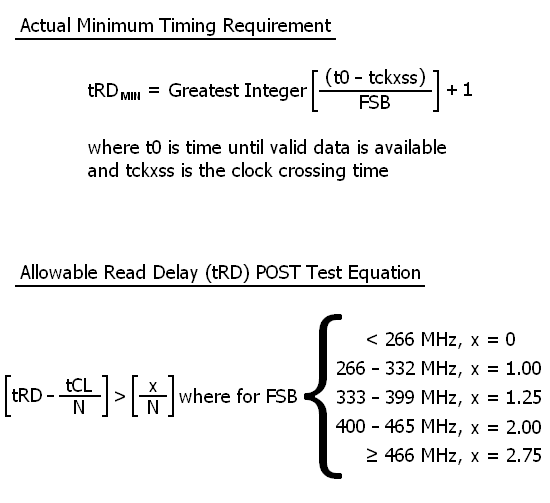
"t0" is the total time it takes data being returned to the CPU as read in memory to cross from the memory bus domain to the system data bus domain. This is dependent on a number of variables, including memory burst length (4 or 8 cycles), Command Rate (1N or 2N), the memory divider in use, CAS (tCL) timing, and the current FSB. "tckxss" is a little more esoteric in nature and is outside the scope of this discussion; the value is generally very small when compared to "t0". The difference in these times, rounded to the lowest integer plus one, bounds the lowest potential tRD setting necessary for data to be properly transferred from one bus to the other.
Because the first expression is too difficult to warrant everyday use, we spent many hours populating a large test matrix table created for recording the POST (Power On Self Test) results of every strap/divider/FSB/CAS setting combination that our test bench was physically capable of supporting. Using this data, we then developed the method and equation you see above, which can determine whether or not a desired memory subsystem configuration will work. It is possible, and rather probable, that there is another step discontinuity in the logic for FSB speeds in excess of the high value in our test range (466MHz). We will leave the discovery of some such value up to others - unless Intel is kind enough to send us additional 45nm dual-core processors, in which case further testing on our part might be justified.
Entering arguments for the use of the "POST Test Equation" are as follows: tRD, in clocks; tCL (CAS), in clocks; FSB, in megahertz (MHz); N, the memory divider in use, expressed in fractional form (i.e. 3:2 would be 3/2); and "x", which should be chosen from the options provided, depending on the FSB in use. Evaluate the left and right side of the equation separately. The expression is satisfied if the left (actual margin) is greater than but not equal to the right (the minimum required margin).
There are no units purposefully associated with these numbers, as this equation is intended as nothing more than a test to determine whether a system will POST using the desired parameters. If the expression is false, the configuration/system will fail to boot; if it is true then the configuration is allowed and the POST event should at least occur. Keep in mind that this equation provides absolutely no assurance that the system will be stable at the settings provided - just because you want to run your memory at DDR2-1200 CAS 3 and the equation says this is possible, does not mean that your wish will be fulfilled. Let's go through a quick exercise of what we have learned regarding the proper use of the "POST Test Equation" with a few practical examples.
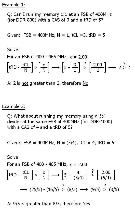
If you can follow these examples then you are ready to move on to the next step - determining optimal system performance points and then validating your results. There are many choices when it comes to deciding how to configure a system for the best possible experience. Some choices are clearly better while other decisions may come to down to personal preference. For instance, some users may be willing to subject their expensive hardware components to higher voltages, creating an environment of accelerated wear and earlier failure. Others may be far less concerned with the consequences of their choices; in either case the trade-offs will be clear. We will now take what we have learned and provide our rationale for why we would feel one overclocking approach to be superior to another. After all, overclocking should always be based on an intelligent decision making process and not the clumsy application of brute-force.


73 Comments
View All Comments
Orthogonal - Friday, January 25, 2008 - link
Just so I understand this correctly, due to the path the data and clocks must travel throughout the devices as explained on page 5, even though you can increase the bandwidth of the Memory modules, the MCH is ultimately the "bottleneck". Historically we falsely assumed higher bandwidth and lower CAS latency translated to better data throughput, but since tRD increased along with it, it was essentially wiped out or unused bandwidth. Now we try to lower tRD as low as possible to reduce MCH latency as it performs the "Clock crossing procedure", which is why the 400Mhz FSB with the lowest tRD latency gives the best data throughput.Also, does this mean that in your "Best Pick" DDR2 configuration summary that the two A+ choices highlighted in Green will effectively result in about the same performance since even though DDR2-1200 has more bandwidth than DDR2-1000, since the tRD=5, they will have the same Trd Delay (12.5ns).
Aivas47a - Friday, January 25, 2008 - link
I'm glad to see Asus implementing these new memory phase adjustment options in the bios. Now if they would provide a greater ability to fine-tune GTL reference voltages I would be a happy camper. GTL is a key setting for quad core overclocking success as Raja has helpfully explained in his DFI P35 review. The selectable percentages Asus currently provides are too crude and don't go high enough.mrlobber - Friday, January 25, 2008 - link
FCG, your article just flat out rocks, thanks for this one, we needed it badly :)One question about the previous Asus boards: X38 and also P35, which lack the exact tRD manipulation, providing the Transaction Booster stuff instead. As far as I understand, your analysis about the default tRD values set by different default fsb and memory divider combinations could also be used to determine the starting tRD value at least for the X38 chipset as well in a pretty straightforward way, and from that point being able to offset the tRD with Transaction Booster up or down to control it as necessary? (P35 would have different default tRD's, but the underlying principles should stay the same?)
And, by making appropriate changes in x values if needed, your POST / no POST inequality should stay applicable as well, right?
kjboughton - Friday, January 25, 2008 - link
All true, although we did talk about how these straps at one time had default tRD values associated with them, the difference has become that these default values are now usually based on the real underlying requirements, such as FSB. Now, exactly how each motherboard vendor sets up and implements this value has a lot to do with how their motherboard falls out in comparison testing. With that being said, boards that perform better generally make use of lower tRD values by default. And because X48 is a speed-binned version of X38, which is superior to P35 with it comes to MCH overclocking, it is also safe to say that the higher-end chipsets will allower the same (or lower) tRD values at FSB levels where the other chipsets may fall flat on their faces. Make sense?Regarding the 'Test POST Equation' - absolutely, I know those equations to be true for X38/X48 but I wouldn't doubt if they ended up being exactly the same for say, P35. A little bit of testing should validate this assumption... ;)
Orthogonal - Friday, January 25, 2008 - link
Can we expect a similar analysis and optimization of strappings, timings etc... when an X48 DDR3 compatible board is released?kjboughton - Friday, January 25, 2008 - link
Yes, the will be an easy bridge to make. DDR3 is very similar to DDR2 and in a lot of respects is a simply extension of the logic already developed. In any case, we will provide this information for reference when the time comes.daddyo323 - Friday, January 25, 2008 - link
I've overclocked a couple cpus before, and each time, I had stability problems due to memory.I have built many systems, but since gave up on overclocking... these new Cores and chipsets look like they were made for it...
My question is, was that CPU stable at 4ghz, and could we have a chart on which settings to set, exactly... I wonder how far we can push this platform with the air cooling.
kjboughton - Friday, January 25, 2008 - link
Everything you want to know, about more, about this CPU can be seen here: http://www.anandtech.com/cpuchipsets/intel/showdoc...">http://www.anandtech.com/cpuchipsets/intel/showdoc...We used the same CPU that can be read about in the above review. The short answer is yes, we were completely stable at 4GHz with just 1.28V real under load.
Cheers,
Kris
Quiksilver - Friday, January 25, 2008 - link
Has there been an ETA on the release date of the X48 chipset? I thought they were supposed to come out in December but they never appeared and this would be the second X48 preview I've seen for AT. Also I remember seeing a flow chart somewhere that had DDR2 & DDR3 being the differences between X38 and X48 of which X38 had both but now it seems X48 has DDR2 as well but will the DDR2 boards be available at launch or are they coming later on?Gary Key - Friday, January 25, 2008 - link
ASUS is telling us mid-February for the X48 launch now. Gigabyte and MSI have confirmed that also, but we have had dates confirmed about a dozen times over the last two months and it always seems to change about three days before the next "official" launch. ;)