The Era of Tera: Intel Reveals more about 80-core CPU
by Anand Lal Shimpi on February 11, 2007 5:44 PM EST- Posted in
- CPUs
The Architecture
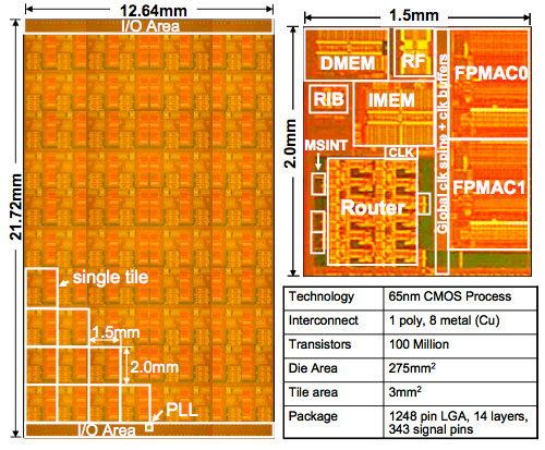
Despite being built on a large die, the individual tiles in the Teraflops chip are extremely simple cores. These aren't x86 cores, although Intel indicated that one of the next steps for the project was to integrate x86 cores. At a high level, each tile is composed of a Processing Engine (PE) to handle all computations and a 5-port router to pass data from one tile to the next.
In order to keep the tile hardware as simple as possible, the tiles are based on a 96-bit Very Long Instruction Word (VLIW) architecture. Intel's other famous VLIW architecture is of course the Itanium, but there's very little else that's in common between the two designs. In short, a VLIW architecture simplifies hardware design by relying on the compiler to schedule instructions for execution rather than having the CPU figure out how to dynamically parallelize and schedule operations. VLIW isn't common for desktop architectures, but for specialized applications it's not far fetched. The number of applications you've got to run on these things is limited, and thus adding complexity on the compiler side isn't such a bad tradeoff.
There are obvious drawbacks to going with a VLIW architecture, but it appears that Intel's fundamental goals with the teraflops chip were to deal with implementing a many-core CPU and not necessarily deliver a high performance one.
The processing engine is composed of a 3KB single-cycle instruction memory, 2KB data memory, 10-port register file, and two single-cycle throughput single-precision floating point multiply-accumulator units.
A maximum of 8 operations can be encoded in a single VLIW instruction on the teraflops chip. Those operations can be FPMACs, loads/stores, as well as instructions to the router on each tile as each tile can pass data and instructions on to any adjacent tile.
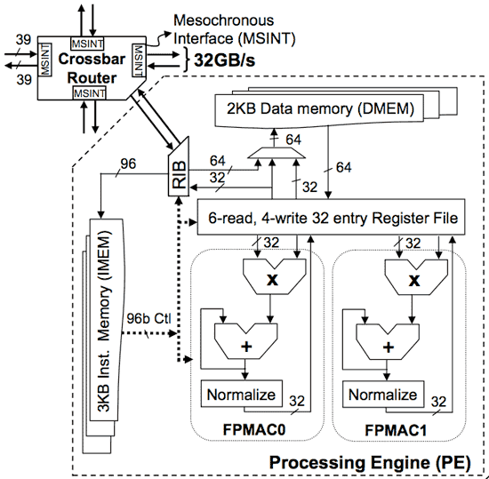
Although the chip itself is capable of processing over one trillion floating point operations per second, don't be fooled by the numbers; these aren't 128-bit FP operations but rather single-precision FP operations. Each tile features two fully pipelined 32-bit floating point multiple-accumulator (FPMAC) units. There are no other execution units on each tile, so all arithmetic operations must be carried out through these FPMACs. This obviously limits the applications that the teraflops chip can be used in, but it also supports the idea that the point of this chip isn't to break speed barriers, but rather develop a framework to introduce other more capable processors with many cores. The real focus here isn't on the floating point throughput of the array of tiles; instead, the primary objective is to work on the network that connects the tiles together.


25 Comments
View All Comments
Navitron - Monday, February 12, 2007 - link
In the words of bill gates "No one will need more than 637 kb of memory for a personal computer." You sound just like him :P Don't bash the technology just because "right now" we don't need it. But what about in 10-20 years, you still think your core 2 duo is gonna cut it in 15 years? Can a IBM 80386 run doom 3? will todays AMD and Intels run -insert game here- 10 years from now.So don't assume just because we don't need it now doesn't mean we wont need it in 3 years.
cscpianoman - Sunday, February 11, 2007 - link
The average consumer might not need it, but large industries will be grabbing at these things faster than you can imagine. Think of health care, for example, the trend is to move towards genetic manipulations/prescreening. These industries want to download a person's entire genetic information, process it, and return it to you with the results of Alzhiemer's, cancer, and heart problems in a matter of minutes. Furthermore, the entertainment industry would love to create more special effects and render them that much faster. I'm sure if they could Pixar would already be placing an order for these. There are hundreds of applications out there that require the power and capability of multi-cores. Sure the consumer may not need it, but the consumer only accounts for less than approx. 5% of what Intel, AMD or whoever makes.mino - Sunday, February 11, 2007 - link
They need it (to sell). Period.Justin Case - Sunday, February 11, 2007 - link
In other words, Intel is doing the same that IBM and AMD (with Cell and Torrenza + Fusion), only with some made-up numbers and more Powerpoint charts. Unless they vastly improve their compilers' paralellization, or come up with a full suite of software optimized for multi-core chips (80? It's hard enough to take full advantage of 4!), this will remain something that "can be done", but which most people will have no use for.joex444 - Sunday, February 11, 2007 - link
attack switch