Abit AT8: µGuru comes to the RD480
by Gary Key on March 10, 2006 12:05 AM EST- Posted in
- Motherboards
Abit AT8: Features
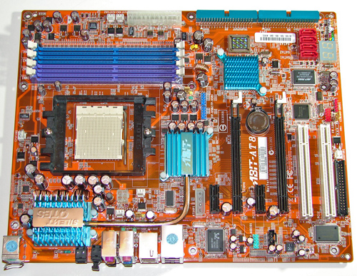
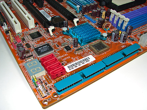
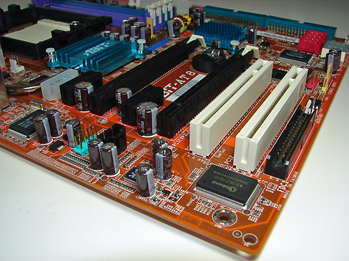
The ULi SATA ports are conveniently located above the number two IDE port connector and to the right of the CP80P post port debug LED. The SATA ports feature the new clamp and latch design, but are not color-coded. The chassis panel is located on the bottom left edge of the board below the CP80P LED. We do miss the power on and reset buttons from previous Abit boards.
The µGuru chipset is located above the ULi SATA ports and independently controls the µGuru functions . The TI TSB43AB22 IEEE 1394 chipset is located above the µGuru chipset. The IEEE 1394 connector is color-coded red and is located directly to the left of the TI IEEE 1394 chipset. The yellow clear CMOS jumper block is a traditional jumper design located to the left of the IEEE 1394 connector and along the edge of the motherboard. The red GURU connector is located below the CMOS jumper and also along the edge of the motherboard.
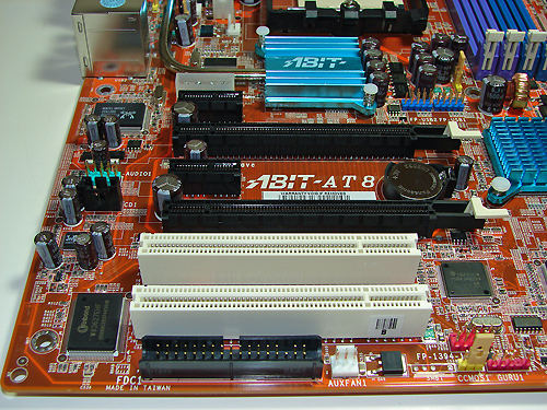
The first PCI Express x1 connector is located below the 4-pin power connector that must be used if two video cards are installed. The first physical PCI Express x16 connector is located next, followed by the second PCI Express x1 connector, second PCI Express x16 connector, and the two PCI 2.3 slots. The floppy drive connector is located below the second PCI slot and is inconveniently located for most case designs. The third of six fan headers located on the board is located to the right of the floppy drive connector.
We did not have any issues installing our ATI X1900XT video cards in the first and second x16 PCI Express slots. These dual slot configuration cards will physically render the second PCI Express x1 and first 32-bit PCI slot useless. We did not have any issues utilizing these slots with video cards containing single slot cooling systems. The first PCI Express x16 connector is considered to be the secondary slot and the second PCI Express x16 connector is considered to be the primary slot. If you utilize one video card, it must be installed in the primary slot. Abit ships a shadow card to use in the secondary slot in single video card configurations, but we found that it was not necessary to use the card. When we installed our EVGA 7800GTX 512MB card in the primary slot, it blocked the first three SATA ports.
The ATI Crossfire Xpress 200 chipset is passively cooled with a small heat sink unit that did not interfere with any installed peripherals. This unit along with the heatpipe running to the large PVM heat sink kept the chipsets cooled well during overclock testing.
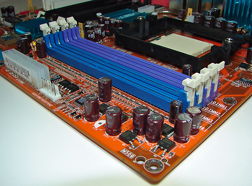
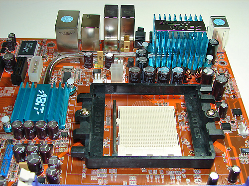
Abit places the ATX12V auxiliary power connector at the top of the CPU socket area. This connector is located in an unusual position and could hamper airflow with cabling that crosses directly over the CPU heat sink/fan; although, we did not have any issues in our case.
The ULi SATA ports are conveniently located above the number two IDE port connector and to the right of the CP80P post port debug LED. The SATA ports feature the new clamp and latch design, but are not color-coded. The chassis panel is located on the bottom left edge of the board below the CP80P LED. We do miss the power on and reset buttons from previous Abit boards.
The µGuru chipset is located above the ULi SATA ports and independently controls the µGuru functions . The TI TSB43AB22 IEEE 1394 chipset is located above the µGuru chipset. The IEEE 1394 connector is color-coded red and is located directly to the left of the TI IEEE 1394 chipset. The yellow clear CMOS jumper block is a traditional jumper design located to the left of the IEEE 1394 connector and along the edge of the motherboard. The red GURU connector is located below the CMOS jumper and also along the edge of the motherboard.
The first PCI Express x1 connector is located below the 4-pin power connector that must be used if two video cards are installed. The first physical PCI Express x16 connector is located next, followed by the second PCI Express x1 connector, second PCI Express x16 connector, and the two PCI 2.3 slots. The floppy drive connector is located below the second PCI slot and is inconveniently located for most case designs. The third of six fan headers located on the board is located to the right of the floppy drive connector.
We did not have any issues installing our ATI X1900XT video cards in the first and second x16 PCI Express slots. These dual slot configuration cards will physically render the second PCI Express x1 and first 32-bit PCI slot useless. We did not have any issues utilizing these slots with video cards containing single slot cooling systems. The first PCI Express x16 connector is considered to be the secondary slot and the second PCI Express x16 connector is considered to be the primary slot. If you utilize one video card, it must be installed in the primary slot. Abit ships a shadow card to use in the secondary slot in single video card configurations, but we found that it was not necessary to use the card. When we installed our EVGA 7800GTX 512MB card in the primary slot, it blocked the first three SATA ports.
The ATI Crossfire Xpress 200 chipset is passively cooled with a small heat sink unit that did not interfere with any installed peripherals. This unit along with the heatpipe running to the large PVM heat sink kept the chipsets cooled well during overclock testing.
Abit places the ATX12V auxiliary power connector at the top of the CPU socket area. This connector is located in an unusual position and could hamper airflow with cabling that crosses directly over the CPU heat sink/fan; although, we did not have any issues in our case.


42 Comments
View All Comments
Gary Key - Friday, March 10, 2006 - link
Abit plans on this board becoming a value performance leader with the AT8-32x being slightly more upscale in the price range. We will be reviewing this board once it is available. However, given the current price range of the RD580 boards, the RD480 boards are the better value at this time given the incremental performance differences of the RD580 (although this would be my personal choice).
There have been some growing pains with the ATI chipsets but there were also growing pains with the NVIDIA/SIS/VIA/ULi/ALI/Intel/etc. chipsets at product launches also. :) Overall, both the ATI RD480 and RD580 are very good chipsets, the fact the SB600 Southbridge was not available in time for either product launch is where I think ATI failed. This forced the board suppliers to utilize a Southbridge solution (ULi M1575) that was not designed in conjunction with the RD480/580 Northbridge. While it is an excellent Southbridge solution, some of the storage access and timing issues that have been reported and now solved, were not seen on the few SB450 equipped boards. I personally expect the ATI equipped boards to mature quickly and provide an excellent competitive alternative to the nForce boards. This is good for all of us.
n7 - Friday, March 10, 2006 - link
Even with the OCing issues, this is still a far better value Crossfire choice for anyone than the craptastic A8R-MVP