Arm Unveils 2023 Mobile CPU Core Designs: Cortex-X4, A720, and A520 - the Armv9.2 Family
by Gavin Bonshor on May 28, 2023 8:30 PM ESTNew DSU-120: More L3 Cache, Doubling Down on Efficiency
For the launch of its Armv9.2 architecture, Arm has decided to opt for a new core complex design for its TCS23 CPU cores by building upon the foundations of its current DSU-110 block. Initially introduced in 2017 along with the Cortex A75 and A55 cores, DSU-110 represented a significant redesign and generational shift to integrate larger pools of shared L3 cache, bandwidth, and scalability. Along with the efficiency tweaking Arm has done to its new Cortex-X4, Cortex-A720, and A520 cores, the new DynamIQ Shared Unit-120 (DSU-120) also plays a significant role in these advancements.
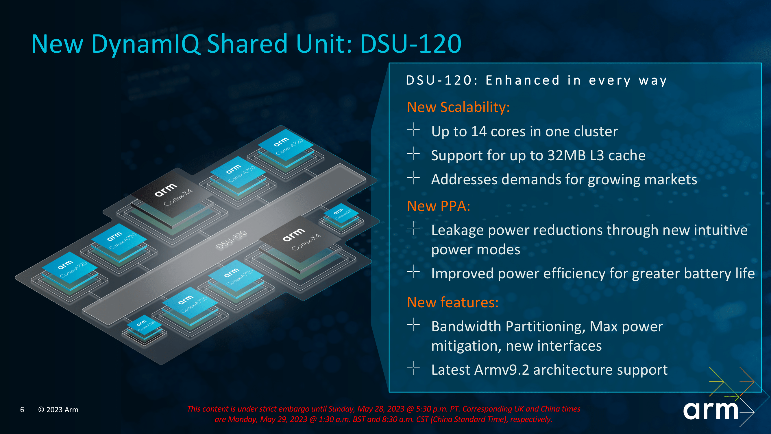
Building a more refined DSU instead of another ground-up design, Arm has made plenty of inroads to improving overall scalability, efficiency, and performance with its DSU-120. Some of the most notable improvements include support for up to 14 CPU cores in a single cluster, which allows SoC vendors to pick and choose their core cluster configurations to suit the device going to market. Arm has also improved its Power and Performance Area (PPA) by implementing new power-saving modes, including RAM and Slicing power-downs, which work in stages depending on the type of workload and the intensity to reduce the overall power footprint of the cluster.
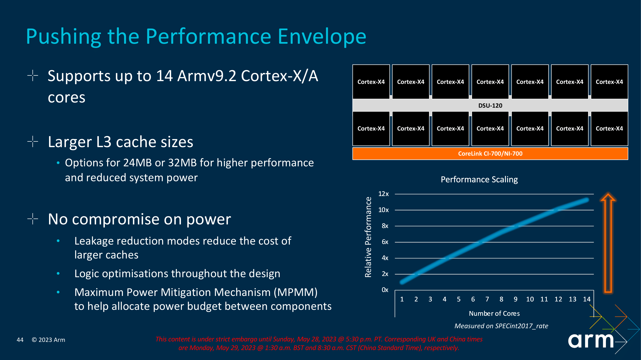
Perhaps the most significant change to DSU-120 from DSU-110 is that Arm has effectively doubled the total amount of shared L3 cache a cluster can implement. DSU-110 initially supported up to 16 MB, whereas DS-120 can now accommodate up to 32 MB of shared L3 cache across the entire complex, with other options also available, including 24 MB. While this isn't a direct implementation into the IP, the decision on the number of L3 cache implemented is entirely down to SoC vendors to decide the right levels of L3 cache based on performance and efficiency balancing depending on the device. The key focus is that DSU-120 and the new TCS23 cluster have the ability to support this if vendors wish to implement more L3 cache.
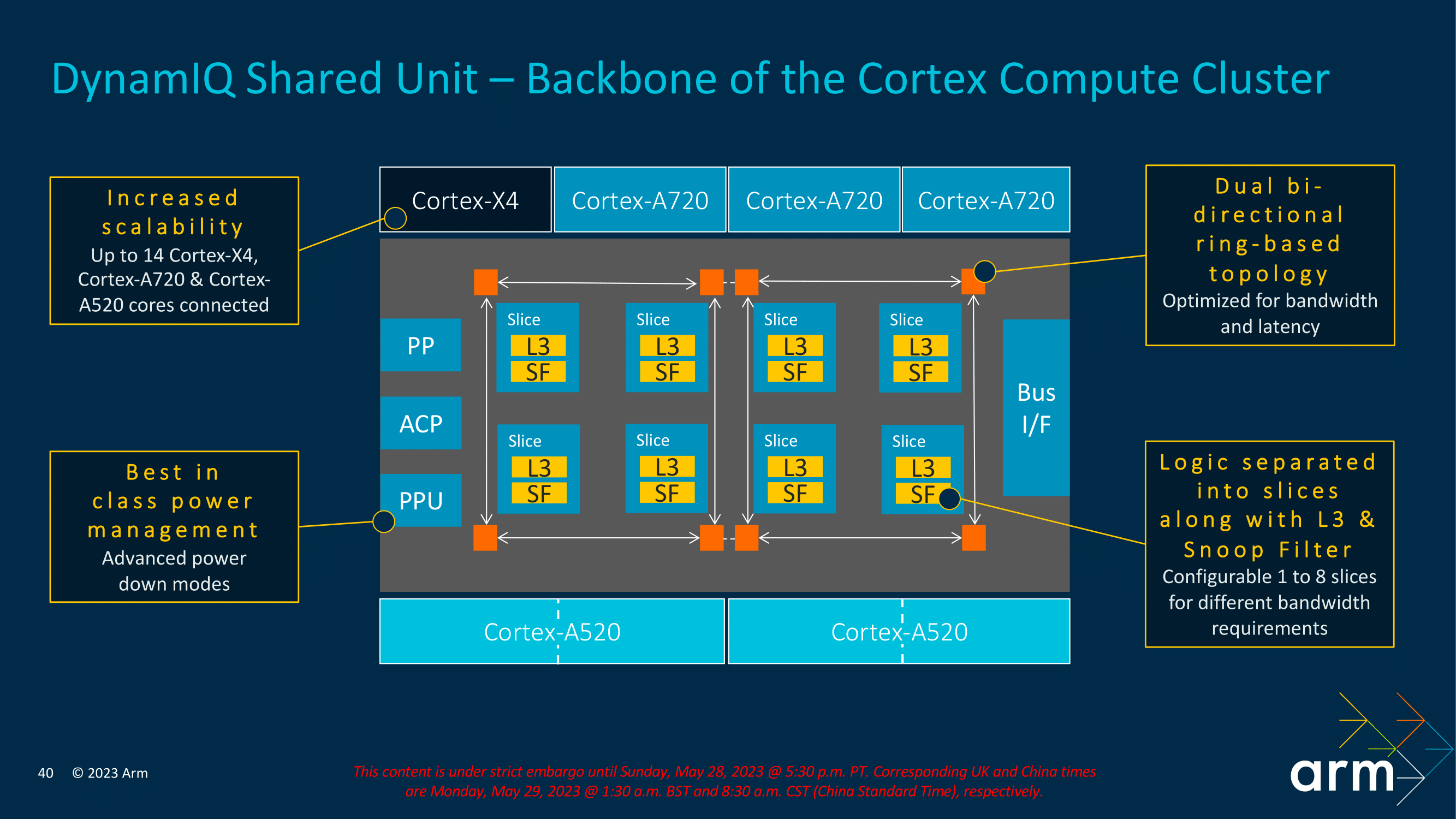
As with the current/previous DSU-110 interconnect, the new DSU-120 also uses a dual bi-directional ring-based topology, which allows data transmission in both directions within the cluster and reduces overall latency. The overall design of the DynamIQ Shared Unit is to optimize things for latency and increase bandwidth, which is precisely what Arm has done by slicing its logic L3 and snoop filters. As such, it is configurable based on specific customer bandwidth requirements. As previously mentioned, DSU-120 allows up to 14 Cortex-X/A cores to be implemented into a cluster, with plenty of benefits of opting for the latest Armv9.2 generation over the previous iterations.
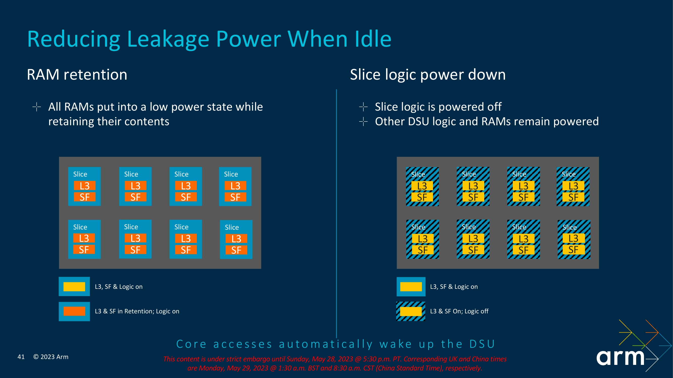
Focusing on the new power improvements to the TCS23 and DSU-120 complex, Arm has identified specific areas where it can save on power to maximize efficiency. One of these is through RAM and reducing any unnecessary power leakage associated with that. To combat this, Arm has opted for a mechanism that allows RAM to be placed into a low-powered state when not being actively used, but still with enough power to ensure the integrity of its contents. The Logic is split into slices with the L3 cache and a snoop filter designed to improve cache coherence within a multi-core complex.
Opting for a sliced approach with snoop filters enables a couple of things. Firstly as we've mentioned, it improves and enhances cache coherence. This means that the cores are fed consistently and up-to-date instructions, and the snoop filter itself is designed to filter out requests that are deemed unnecessary, which does give some efficiency benefits. Secondly, slicing allows Arm's IP to increase scalability, which with an increase in cores, means an increase in slices with dedicated cache slices, allowing for better distribution of data and lower data contention rates. Armv9.2 IP with the DSU-120 allows for between 1 and 8 slices to be used, designed to enable SoC vendors the flexibility to work within their bandwidth requirements.

Arm claims that RAM power-down enabled across half of the L3 RAMs on the complex is suitable for large L3 caches when all of the capacity isn't being used. By allowing RAM power-down, all of the unused RAM is put into a low power state, but with enough to keep the contents and withhold their integrity within the memory substructure. Even with RAM and Slice power-downs active, the cores can still be active and process relevant instructions and data. One slice will effectively remain active, which is ideal for smaller and light workloads on a single core, but when it comes to powering down features on the DSU-120 interconnect, accessing the cores will enact a wake-up of the DSU-120.
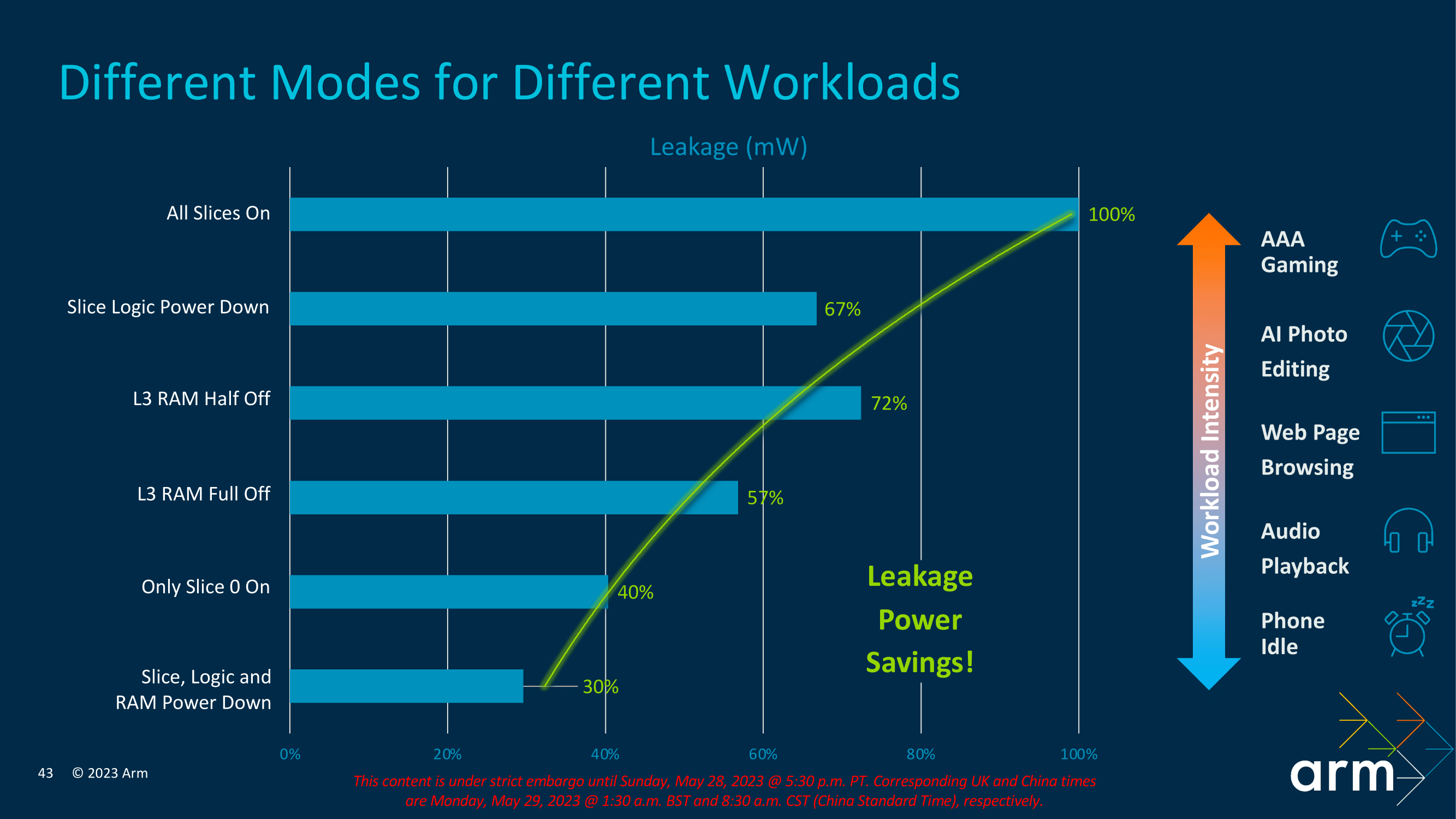
Looking at how this efficiency translates into data, Arm has provided a handy slide with estimates from its own testing. As we can see, with various levels of RAM and Slice Logic power-downs, we get varied potential power savings, which can then be budgeted back into the cores themselves for higher performance levels. Different workloads and tasks require different levels of core power, coherence, intensity, and L3 allocation, so different power-downs lead to varying levels of leakage and power efficiency savings. Arm's figures estimate between 30 and 72% at the other states of power-down, with 100% savings in leakage with all the slices enabled.


52 Comments
View All Comments
Doug_S - Tuesday, May 30, 2023 - link
Yes TSO is a mode, which requires a setting IN THE ISA to be able to enable it. That setting does not exist on ARM CPUs, only on Apple Silicon implementations.abr2 found what I didn't have time to look for in the ARMv8 architecture reference manual proving your ridiculous claim that ARMv8 required AArch32 support was wrong. Now you're picking on nits trying to twist my words as if I was claiming TSO is an instruction. Give it up you are wrong, everyone knows it, go away quietly instead of making yourself look like even a bigger fool.
dotjaz - Tuesday, May 30, 2023 - link
And your understanding of ARMv9 is abysmal at best. ARMv9-A made Aarch32 EL0 optional, it wasn't possible in ARMv8-A. There is no special license or "something like that".Chelgrian - Tuesday, May 30, 2023 - link
It has been possible an architecturally permissible since ARMv8.0 to create an AArch64 only implementation. If AArch32 is not supported at a particular exception level then setting the M[4] bit in the SPSR and executing an ERET instruction to that level will produce an illegal exception return exception. Combined with designing the system to only reset in to AArch64 at the highest implemented exception level gives you an AArch64 only design.This tangentially referred to in rule R-tytwb in section D1.3.4 of revision J.a of the ARM Architecture Reference Manual.
A conformant ARMv8.x implementation can (but it not mandated to) implement AArch32 at any exception level.
A conformant ARMv9.x implementation may only implement AArch32 at EL0. This is documented in section 3.1 of revision J.a of the ARM Architecture Reference Manual.
There are even documented ARMv8.1 processors out there which are AArch64 only for example the Cavium ThunderX2
https://en.wikichip.org/wiki/cavium/thunderx2
"Only the 64-bit AArch64 execution state is support. No 32-bit AArch32 support."
abr2 - Tuesday, May 30, 2023 - link
From:Arm® Architecture Reference Manual
Armv8, for Armv8-A architecture profile
[2021 version]
D1.20.2 Support for Exception levels and Execution states
Subject to the interprocessing rules defined in Interprocessing on page D1-2525, an implementation of the Arm architecture could support:
• AArch64 state only.
• AArch64 and AArch32 states.
• AArch32 state only.
techconc - Thursday, June 8, 2023 - link
@dotjaz - You don’t know what you’re talking about. The Apple A7 chip supported both A32 and A64 instruction set. By the A11 (in 2017), Apple dropped A32 instruction set and was 64bit only.dotjaz - Tuesday, May 30, 2023 - link
> I'm very fairly certain of this, but if you know something I don't? (I might not..)You are clearly wrong, no ARM licensees can alter ARM ISA in any way. That's the fundation of ARM's licensing terms. And that's the sole reason Apple's AMX extention is masked as undocumented "co-processor" not available to anyone. Even if you knew nothing about the fundamental licensing terms, you should be able to figure that out because if this.
name99 - Monday, May 29, 2023 - link
Jesus. The levels of delusion that are required to write a comment like this.You really think that
(a) ARM is going to make a big deal about Apple being, in some legalistic sense, "non-compliant" AND
(b) that Apple gives a fsck?
Exactly who do you think gets hurt if Apple are not allowed to call APPLE SILICON (note that branding...) Arm Compliant?
Wereweeb - Tuesday, May 30, 2023 - link
Lmao apple fanboys still as hilarious and ignorant as alwaysSilver5urfer - Sunday, May 28, 2023 - link
So much of this nonsensical 64Bit bs. Esp in the name of security, News Flash - Qualcomm EDL mode exists and thankfully it helps the folks to unlock their Bootloaders.The whole 64Bit thing killed the passion on Android. Google just enforces it brutally by n-1 where n being the latest API SDK, thus making all the old apps go obsolete. Windows and x86 excels massively just because of this, Apple did it because they always want to control everything which they do, and the stupid Google just copies them in hoping to make same but they killed all fun on android now, the UI is so boring garbage and the whole Filesystem nerfs - Scoped Storage, lack of proepr SD Card app support and a ton of other APIs blacklisted. Limited the scope of foreground and background apps utilizing the hardware of a phone.
What's the use of the ARM processor devices, when your latest and greatest X4 ARM phone will be outdated in 1 year and goes to dumpster after 2-3 years max. Non Removable, non serviceable, no longevity of the OS / HW / Software. Locked like chastity belt for the User tinkering when the core OS, the Kernel runs Linux. A big L to consumers and all that Environment jabber is literally just a worthless cacophony. Literally you have latest V30 class Micro SDs and SD Association even had PCIe / NVMe SSD class but since not a single $1000-$2000 Android phone pushes forward for a real computer in pocket, its rather a spybox and a mere 2FA device with some Navigation, Social Media, Camera attached.
All this ARM tech is only useful if your device Software API can open it up properly and used a proper pocket computer. But that ship has sailed. All that X4 processing power and multi core non homogeneous compute wasted on basic consumables.
rpg1966 - Monday, May 29, 2023 - link
Could you explain how the UI is affected by the bitness of the OS?