NVIDIA Announces H100 NVL - Max Memory Server Card for Large Language Models
by Ryan Smith on March 21, 2023 12:15 PM EST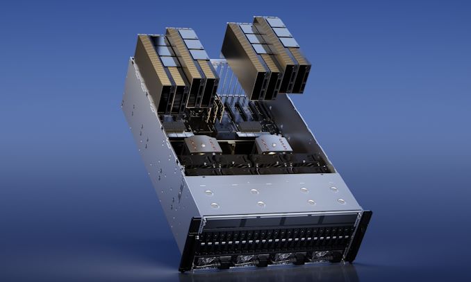
While this year’s Spring GTC event doesn’t feature any new GPUs or GPU architectures from NVIDIA, the company is still in the process of rolling out new products based on the Hopper and Ada Lovelace GPUs its introduced in the past year. At the high-end of the market, the company today is announcing a new H100 accelerator variant specifically aimed at large language model users: the H100 NVL.
The H100 NVL is an interesting variant on NVIDIA’s H100 PCIe card that, in a sign of the times and NVIDIA’s extensive success in the AI field, is aimed at a singular market: large language model (LLM) deployment. There are a few things that make this card atypical from NVIDIA’s usual server fare – not the least of which is that it’s 2 H100 PCIe boards that come already bridged together – but the big takeaway is the big memory capacity. The combined dual-GPU card offers 188GB of HBM3 memory – 94GB per card – offering more memory per GPU than any other NVIDIA part to date, even within the H100 family.
| NVIDIA H100 Accelerator Specification Comparison | |||||
| H100 NVL | H100 PCIe | H100 SXM | |||
| FP32 CUDA Cores | 2 x 16896? | 14592 | 16896 | ||
| Tensor Cores | 2 x 528? | 456 | 528 | ||
| Boost Clock | 1.98GHz? | 1.75GHz | 1.98GHz | ||
| Memory Clock | ~5.1Gbps HBM3 | 3.2Gbps HBM2e | 5.23Gbps HBM3 | ||
| Memory Bus Width | 6144-bit | 5120-bit | 5120-bit | ||
| Memory Bandwidth | 2 x 3.9TB/sec | 2TB/sec | 3.35TB/sec | ||
| VRAM | 2 x 94GB (188GB) | 80GB | 80GB | ||
| FP32 Vector | 2 x 67 TFLOPS? | 51 TFLOPS | 67 TFLOPS | ||
| FP64 Vector | 2 x 34 TFLOPS? | 26 TFLOPS | 34 TFLOPS | ||
| INT8 Tensor | 2 x 1980 TOPS | 1513 TOPS | 1980 TOPS | ||
| FP16 Tensor | 2 x 990 TFLOPS | 756 TFLOPS | 990 TFLOPS | ||
| TF32 Tensor | 2 x 495 TFLOPS | 378 TFLOPS | 495 TFLOPS | ||
| FP64 Tensor | 2 x 67 TFLOPS? | 51 TFLOPS | 67 TFLOPS | ||
| Interconnect | NVLink 4 (600GB/sec) |
NVLink 4 (600GB/sec) |
NVLink 4 18 Links (900GB/sec) |
||
| GPU | 2 x GH100 (814mm2) |
GH100 (814mm2) |
GH100 (814mm2) |
||
| Transistor Count | 2 x 80B | 80B | 80B | ||
| TDP | 700-800W | 350W | 700W | ||
| Manufacturing Process | TSMC 4N | TSMC 4N | TSMC 4N | ||
| Interface | 2 x PCIe 5.0 (Quad Slot) |
PCIe 5.0 (Dual Slot) |
SXM5 | ||
| Architecture | Hopper | Hopper | Hopper | ||
Driving this SKU is a specific niche: memory capacity. Large language models like the GPT family are in many respects memory capacity bound, as they’ll quickly fill up even an H100 accelerator in order to hold all of their parameters (175B in the case of the largest GPT-3 models). As a result, NVIDIA has opted to scrape together a new H100 SKU that offers a bit more memory per GPU than their usual H100 parts, which top out at 80GB per GPU.
Under the hood, what we’re looking at is essentially a special bin of the GH100 GPU that’s being placed on a PCIe card. All GH100 GPUs come with 6 stacks of HBM memory – either HBM2e or HBM3 – with a capacity of 16GB per stack. However for yield reasons, NVIDIA only ships their regular H100 parts with 5 of the 6 HBM stacks enabled. So while there is nominally 96GB of VRAM on each GPU, only 80GB is available on regular SKUs.

The H100 NVL, in turn, is the mythical fully-enabled SKU with all 6 stacks enabled. By turning on the 6th HBM stack, NVIDIA is able to access the additional memory and additional memory bandwidth that it affords. It will have some material impact on yields – how much is a closely guarded NVIDIA secret – but the LLM market is apparently big enough and willing to pay a high enough premium for nearly perfect GH100 packages to make it worth NVIDIA’s while.
Even then, it should be noted that customers aren’t getting access to quite all 96GB per card. Rather, at a total capacity of 188GB of memory, they’re getting effectively 94GB per card. NVIDIA hasn’t gone into detail on this design quirk in our pre-briefing ahead of today’s keynote, but we suspect this is also for yield reasons, giving NVIDIA some slack to disable bad cells (or layers) within the HBM3 memory stacks. The net result is that the new SKU offers 14GB more memory per GH100 GPU, a 17.5% memory increase. Meanwhile the aggregate memory bandwidth for the card stands at 7.8TB/second, which works out to 3.9TB/second for the individual boards.
Besides the memory capacity increase, in a lot of ways the individual cards within the larger dual-GPU/dual-card H100 NVL look a lot like the SXM5 version of the H100 placed on a PCIe card. Whereas the normal H100 PCIe is hamstrung some by the use of slower HBM2e memory, fewer active SMs/tensor cores, and lower clockspeeds, the tensor core performance figures NVIDIA is quoting for the H100 NVL are all at parity with the H100 SXM5, indicating that this card isn’t further cut back like the normal PCIe card. We’re still waiting on the final, complete specifications for the product, but assuming everything here is as presented, then the GH100s going into the H100 NVL would represent the highest binned GH100s currently available.
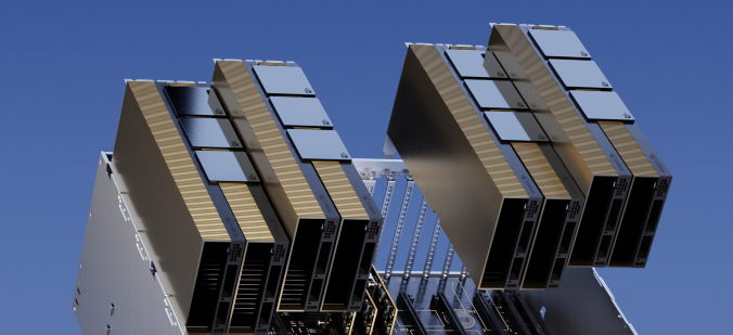
And an emphasis on the plural is called for here. As noted earlier, the H100 NVL is not a single GPU part, but rather it’s a dual-GPU/dual-card part, and it presents itself to the host system as such. The hardware itself is based on two PCIe form-factor H100s that are strapped together using three NVLink 4 bridges. Physically, this is virtually identical to NVIDIA’s existing H100 PCIe design – which can already be paired up using NVLink bridges – so the difference isn’t in the construction of the two board/four slot behemoth, but rather the quality of the silicon within. Put another way, you can strap together regular H100 PCie cards today, but it wouldn’t match the memory bandwidth, memory capacity, or tensor throughput of the H100 NVL.
Surprisingly, despite the stellar specs, TDPs remain almost. The H100 NVL is a 700W to 800W part, which breaks down to 350W to 400W per board, the lower bound of which is the same TDP as the regular H100 PCIe. In this case NVIDIA looks to be prioritizing compatibility over peak performance, as few server chassis can handle PCIe cards over 350W (and fewer still over 400W), meaning that TDPs need to stand pat. Still, given the higher performance figures and memory bandwidth, it’s unclear how NVIDIA is affording the extra performance. Power binning can go a long way here, but it may also be a case where NVIDIA is giving the card a higher than usual boost clockspeed since the target market is primarily concerned with tensor performance and is not going to be lighting up the entire GPU at once.
Otherwise, NVIDIA’s decision to release what’s essentially the best H100 bin is an unusual choice given their general preference for SXM parts, but it’s a decision that makes sense in context of what LLM customers need. Large SXM-based H100 clusters can easily scale up to 8 GPUs, but the amount of NVLink bandwidth available between any two is hamstrung by the need to go through NVSwitches. For just a two GPU configuration, pairing a set of PCIe cards is much more direct, with the fixed link guaranteeing 600GB/second of bandwidth between the cards.
But perhaps more importantly than that is simply a matter of being able to quickly deploy H100 NVL in existing infrastructure. Rather than requiring installing H100 HGX carrier boards specifically built to pair up GPUs, LLM customers can just toss H100 NVLs in new server builds, or as a relatively quick upgrade to existing server builds. NVIDIA is going for a very specific market here, after all, so the normal advantage of SXM (and NVIDIA’s ability to throw its collective weight around) may not apply here.
All told, NVIDIA is touting the H100 NVL as offering 12x the GPT3-175B inference throughput as a last-generation HGX A100 (8 H100 NVLs vs. 8 A100s). Which for customers looking to deploy and scale up their systems for LLM workloads as quickly as possible, is certainly going to be tempting. As noted earlier, H100 NVL doesn’t bring anything new to the table in terms of architectural features – much of the performance boost here comes from the Hopper architecture’s new transformer engines – but the H100 NVL will serve a specific niche as the fastest PCIe H100 option, and the option with the largest GPU memory pool.
Wrapping things up, according to NVIDIA, H100 NVL cards will begin shipping in the second half of this year. The company is not quoting a price, but for what’s essentially a top GH100 bin, we’d expect them to fetch a top price. Especially in light of how the explosion of LLM usage is turning into a new gold rush for the server GPU market.


24 Comments
View All Comments
Ryan Smith - Tuesday, March 21, 2023 - link
The answer to that is however Pytorch would treat a dual H100 setup today. That part is unchanged.p1esk - Tuesday, March 21, 2023 - link
That is disappointing.mode_13h - Wednesday, March 22, 2023 - link
It's not surprising. The 600 GB/s link between cards is a mere 15% of the onboard bandwidth. If software naively treated it as a single GPU, performance would be garbage.Conversely, I'm sure it's now well-supported for software to divide up big networks across multiple GPUs and align the division with a layer boundary. If you do it that way, the NVLink is probably no bottleneck at all.
abufrejoval - Wednesday, April 19, 2023 - link
While I understand your sentiment, it's physics.But playing around with Llama on 2 V100 (which can't do all the nice low precision weight things), I noticed that there was very little noticeable slowdown with the 2nd V100, which in my case only shared the PCIe bus, too.
I guess the explanation is that Llama like the other LLM models are *already* split into many graphs to manage the updates of the weights during training, which happens on thousands of GPUs after all, which connect via Infiniband at best, because there is nothing else readily available to OpenAI.
So the penalty and pain typically associated with models that outgrow a single GPU's memory space have already been worked around as much as possible with the current breed of LLMs and that is why they don't deteriorate as much as you'd think when they are spread for inference, too.
I was even surprised to see how well Llama tolerated having some graphs moved to the CPU as well, where unfortunately my hardware (and the current PyTorch release) don't yet support the lower precision weights (and you can't seem to have mixed weight graphs due to software constraints), but that is about to change going forward, as CPU vendors don't want to loose out on the opportunity and would like to play their RAM size card.
I think I could load the 13B (or 30B?)Llama into 768GB of RAM on a 28 core Skylake, but it was at one letter per second, if that, rather impractical.
30B is much more fun on my RTX3090 with 24GB VRAM and 4-bit weights, and I believe I have seen code for 3-bit weights, too.
Did not get to play around with that, yet.
brucethemoose - Tuesday, March 21, 2023 - link
"12x the GPT3-175B inference throughput"That is a very interesting claim, as GPT-3 is a closed source model with precisely 1 user: OpenAI.
The open source models are kinda being cobbled together into usable repos as I type this.
p1esk - Tuesday, March 21, 2023 - link
The model architecture is well known, it was described in the paper. Weights have not been released, but they are not needed to measure the hw performance.mode_13h - Wednesday, March 22, 2023 - link
And who do you think supplies hardware to OpenAI?p1esk - Wednesday, March 22, 2023 - link
Microsoftmode_13h - Thursday, March 23, 2023 - link
For one thing, they only bought a controlling stake just a couple months ago.I'm talking about the hardware GPT-3 was developed on, last year.
BTW, I'm sure Microsoft is just buying Nvidia GPUs. I've read they're doing stuff with FPGAs, but AFAIK MS has no comparable hardware solution for such large models.
abufrejoval - Wednesday, April 19, 2023 - link
OpenAI is hosted on Azure. Have a look here:https://www.nextplatform.com/2023/03/21/inside-the...