AMD Zen 4 Ryzen 9 7950X and Ryzen 5 7600X Review: Retaking The High-End
by Ryan Smith & Gavin Bonshor on September 26, 2022 9:00 AM ESTDDR5 & AMD EXPO Memory: Memory Overclocking, AMD's Way
The final major feature being introduced with the AM5 platform is DDR5 memory support. Like AM4, which was introduced alongside AMD’s shift over from DDR3 to DDR4, socket AM5 is being rolled out to bring support for DDR5 for the platform.
In fact, socket AM5 only brings DDR5 support. Unlike rival Intel, who opted to support both DDR4 and DDR5 memory with their Alder Lake (12th Gen Core) CPUs, AMD is only supporting DDR5 on the AM5 platform. This is a true platform limitation, and there is no going back.
Like other engineering decisions, this marks a trade-off being made by AMD. In the short term, this is going to drive up the total cost of an AM5 system relative to a theoretical AM5 system with DDR4 memory; DDR5 simply costs more right now. But at the same time, it simplifies things over the long run of the platform, especially since AMD is planning on supporting it through 2025. There will be no such thing as a DDR4 AM5 motherboard, and AMD needs not bake DDR4 support into any of the Ryzen memory controllers.
Ultimately, with AMD starting the DDR5 transition roughly a year after Intel, the company’s expectations are that DDR5 prices are going to continue falling fast enough that they’re going to reach parity with DDR4 before too long. So why implement DDR4 support if it’s only going to be necessary for a short period of time?
As for memory speeds and capacities supported, while AM5 enforces the use of DDR5, ultimately it’s the individual memory controllers that determine the rest. For AMD’s Ryzen 7000 desktop processors, which are based on the Zen 4 Raphael design, these chips offer support for official (JEDEC) speeds at up to DDR5-5200 for a 1 DIMM Per Channel (DPC) configuration. But, like all other DDR5 products we’ve seen thus far, 2 DPC comes with a significant penalty; in that case the maximum JEDEC speed is reduced to just DDR5-3600.
So as was the case with Intel’s Alder Lake platform, system builders are going to need to put a lot more thought into how they go about adding memory, and how they’re going to handle future memory expansion, if at all. While Ryzen 7000 can drive a 2 DPC/4 DIMM setup, you’re going to lose 31% of your memory bandwidth if you go that route. So for peak performance, it’ll be best to treat Ryzen 7000 as a 1 DPC platform.
Meanwhile, for system builders looking at reliability and data integrity as opposed to performance, AMD has confirmed that Ryzen 7000 also supports ECC memory. Unfortunately, the compatibility situation is essentially unchanged from the AM4 platform, which is to say that while the CPU supports ECC memory, it’s going to be up to motherboard manufacturers to properly validate it against their boards. For boards that aren’t doing validation, AMD can’t guarantee ECC is going to work. Though it’s largely a moot point for today’s launch anyhow, since although DDR5 ECC UDIMMs exist, they are in very short supply.
Also, while we didn’t expect it to be supported to begin with, AMD has confirmed that Ryzen 7000 won’t support RDIMMS/LRDIMMs. So it’s unbuffered DIMMs all the way.
Overclocking Memory Ratios
JEDEC standard speeds aside, the Ryzen 7000 series will also support memory overclocking. And thanks to a combination of the switch to DDR5 memory, changes to AMD’s memory controllers, and changes to AMD’s power delivery infrastructure, the rules have changed.
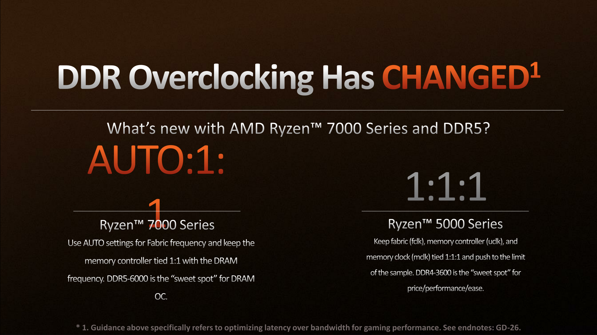
On Ryzen 5000, the ideal configuration for memory overclocking was to run the fabric clock, memory controller, and memory clock all in sync at the same frequencies. This made DDR4-3600 the typical “sweet spot” for the platform, as going faster would typically require running parts of the CPU out of sync so that they could stay within their own attainable clockspeeds.
But for Ryzen 7000, AMD has loosened things up a bit. Ryzen 7000 systems can still get improved memory performance even when the fabric clock is allowed to go out of sync with the memory controller. As a result, most overclockers can just leave that clock set to Auto, and instead focus on keeping the memory and memory controller clocks in sync in a 1:1 ratio.
Specifically, when the fabric clock is set to Auto, it’s typically run at 2000MHz. Meanwhile the memory and memory controller clocks will be running at anywhere between 2400MHz and 3000MHz, depending on the speed of the RAM kit used. Ultimately, the goal for the best performance is to get the fabric clock to 2000MHz and then keep the memory/MC clock at 3000MHz or less. Otherwise, if memory speeds exceed 3000MHz (DDR5-6000), then the memory controller will fall to 1:2 with the memory frequency, which will incur a performance hit.
It should be noted that AMD’s idea of optimal memory speeds here is high memory clocks with low memory latencies, rather than pushing the absolute fastest memory clocks. On good chips it should be possible to drive Ryzen 7000 at speeds above DDR5-6000, but the latency hit from things falling out of sync will be significant – enough so that it’s likely going to be a performance regression for most workloads.
Overclocking with EXPO
But for most users doing memory overclocking, they’re likely going to simply rely on factory overclocked memory kits with pre-programmed profiles. And this is where AMD is rolling out their own standard for those memory kit profiles: EXPO.
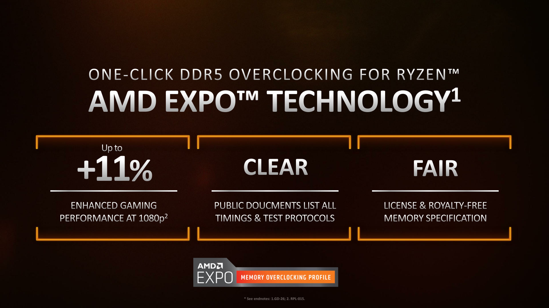
AMD EXPO stands for EXtended Profiles for Overclocking and is designed to provide users with high-end memory overclocking when used in conjunction with AMD's Ryzen 7000 series processors. Similar to Intel's preexisting X.M.P (Extreme Memory Profile) technology found on most consumer-level memory kits designed for desktop Intel platforms, AMD's EXPO technology aims to do the same, but as an open standard with an emphasis on providing the best settings for AMD platforms.
The premise of AMD EXPO is that is a one-click DDR5 overclocking function for AM5 motherboards. On the surface EXPO is essentially a set of X.M.P-like profile specifically designed for AMD's Ryzen 7000 (Zen 4) processors.
The major impetus behind EXPO is two-fold. The first is simple: Intel doesn’t share XMP. There’s no published specification for it, and while AMD has reverse engineered it to some extent, they can’t be sure of what’s going on (especially with DDR5/XMP 3). So rather than deal with the potential compatibility issues and inefficiencies, they’re just going their own way. The second benefit for EXPO being that it means that memory kit manufacturers can then create memory profiles that are AMD-specific, potentially using tighter sub-timings that are possible in conjunction with AMD processors, but not with Intel’s.
It is worth noting that, despite the existence of EXPO, DDR5 memory with X.M.P profiles will be supported on Ryzen 7000 platforms. Still, AMD is very clearly pushing customers towards using EXPO DIMMs with their systems to get the best performance out of AMD systems.
As for EXPO itself, like most other AMD standards, the company is making this an open and royalty free standard (XMP is believed to have royalties, but how much has never been officially published). So memory kit partners will be able to implement EXPO profiles without the blessing of AMD, or needing to pay AMD for the privilege.
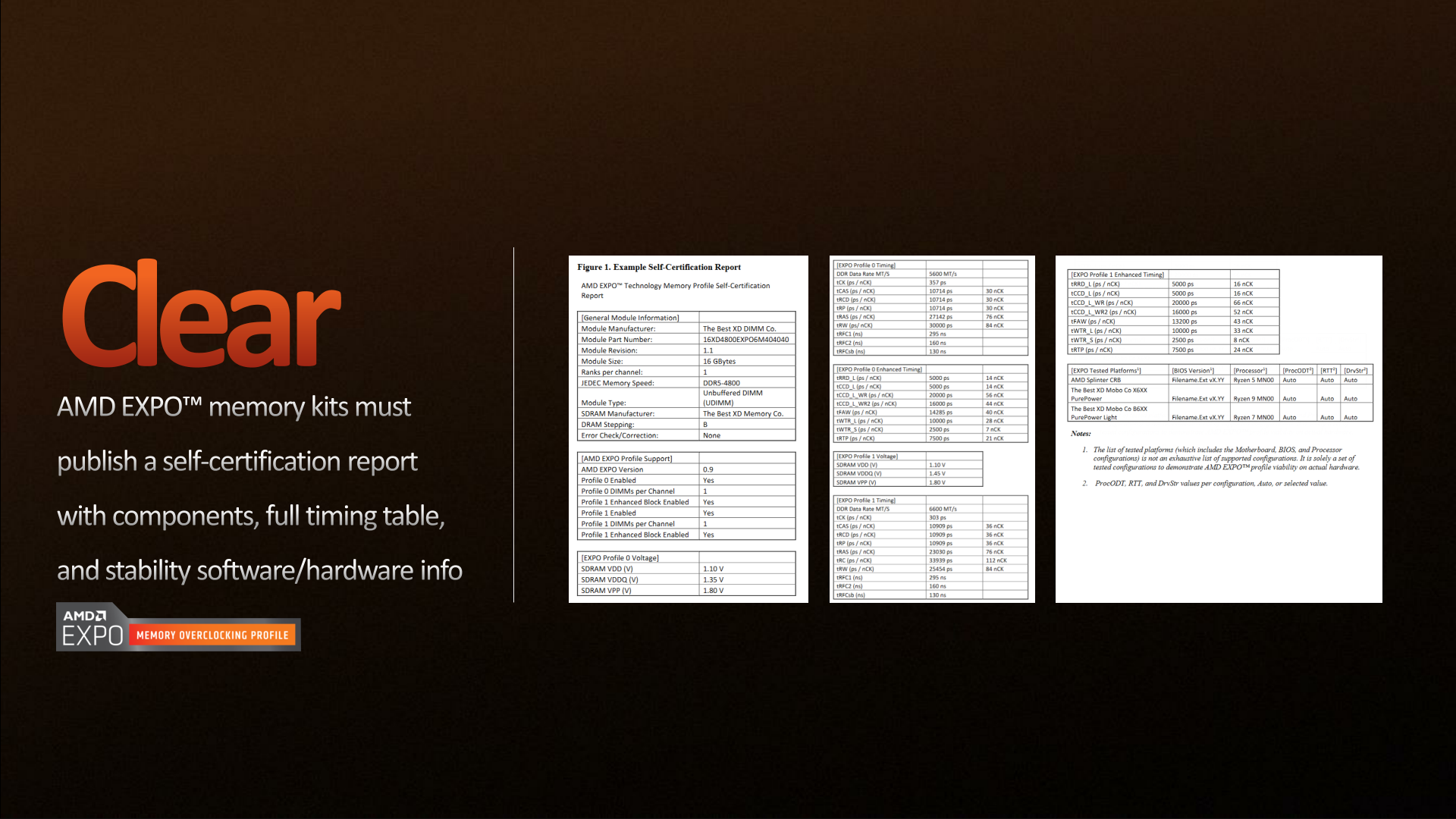
With that said, EXPO will be a self-certification program. So AMD is not charging anything for it, but at the same time they are not doing much in the way of extra work to validate support for it.
In lieu of that, memory kit manufacturers will be required to publish their self-certification reports. These reports will lay out in detail what memory was tested on what systems, and with what timings and voltages. The idea here being that openness goes both ways, and that buyers should be able to see complete configuration settings a profile calls for. The detailed data is in some respects overkill, but it also means that if memory kit manufacturers opt for a high-clocked kit with tight primary timings and loose secondary timings, potential customers will be able to see those full timings in advance.
As with manual memory overclocking, AMD expects the sweet spot for EXPO kits to be DDR5-6000. In an example profile provided for a 2 x 16GB G.Skill memory kit, that kit runs at DDR5-6000 CL30, with a VDD voltage of 1.35v. It’s kits like these that AMD expects to provide the best performance, offering rather low memory latencies in conjunction with a more modest increase in memory frequency.
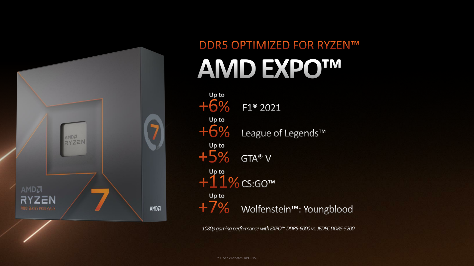
The specific performance gains will vary depending on the workloads. But for gaming tasks, some of the most DRAM latency-sensitive workloads, AMD is touting performance gains of up to 11% at 1080p. Otherwise, at more GPU-limited resolutions and settings, the gains will be understandably lower.


205 Comments
View All Comments
Oxford Guy - Tuesday, September 27, 2022 - link
This has been posted for years. ReplyBoredInPDX - Tuesday, September 27, 2022 - link
I’m confused. I they 720p tests you write:“All gaming tests here were run using integrated graphics, with a variation of 720p resolutions and at minimum settings.”
Yet all the prior-gen AMD CPUs tested are lacking an IGP. Am I missing something? Reply
Ryan Smith - Friday, September 30, 2022 - link
You are not missing anything; we did not run any iGPU tests. That's a bit of boilerplate text that did not get scrubbed from this article. Thanks for bringing it up! ReplyGigaplex - Wednesday, September 28, 2022 - link
There's some odd results here and the article commentary doesn't seem to touch on it. Why is the 7600X absolutely trounced in Geekbench 4.0 MT? The second slowest CPU (3600XT) more than doubles it. And yet the 7950X wins by a mile in that same test, so it shouldn't be architectural. And in some of the gaming tests, the 7600X wins, and in some it comes dead last. ReplyDribble - Wednesday, September 28, 2022 - link
The processors are particularly cache bound - i.e. it fits in cache it runs very fast, if it doesn't it falls off rapidly. That is often visible in games where it'll run amazingly in some (mostly older) games, but tend to fall off, particularly in the lows, in more complex (mostly newer) games. Replyricebunny - Wednesday, September 28, 2022 - link
The SPEC multithreaded tests are N separate instantiations of the single thread tests. That’s a perfect scenario where there is no dependency or serialization in the workload and tells us very little how the CPUs would perform in a parallel workload application. There are SPEC tests specifically designed to test parallel performance, but I do not see them included in this report. Anandtech, can you comment on this? Replyabufrejoval - Wednesday, September 28, 2022 - link
Emerging dGPUs not supporting PCIe 5.0 is just crippleware!While I can easily see that 16 lanes of PCIe 5.0 won't do much for any game, I can very much see what I'd do with the 8 lanes left over when all dGPU bandwidth requirements can be met with just 8 lanes of PCIe 5.0.
Why can't they just be good PCIe citizens and negotiate to use 16 lanes of PCIe 4.0 on lesser or previous generation boards and optimize lane allocation on higher end PCIe 5.0 systems that can then use bifurcation to add say a 100Gbit NIC, plenty of Thunderbolt 4 or better yet, something CXL?
Actually I'd be really astonished if this wasn't even an artifical cap and that the Nvidia chips may actually be able to do PCIe 5.0.
It's just that they'd much rather have people use NVlink. Reply
TheinsanegamerN - Tuesday, October 4, 2022 - link
Um....dude, 4.0x16 and 5.0x8 have the same bandwidth, and no GPU today can saturate 4.0, not even close. The 300ti OCed manages to saturate.....2.0. 3.0 is a whopping 7% faster.You got awhile man. Reply
abufrejoval - Wednesday, September 28, 2022 - link
It should be interesting to see if AMD is opening the architecture for 3rd parties to exploit the actual potential of the Ryzen 7000 chips.The current mainboard/slot era that dates back to the 1981 IBM-PC (or the Apple ][) really is coming to an end and perhaps few things highlight this as well as a 600 Watt GPU that has a 65 Watt mainboard hanging under it.
We may really need something more S100 or VME, for those old enough to understand that.
Thunderbolt cables handle 4 lanes of PCIe 3.0 today and AFAIK cables are used for much higher lane counts and PCIe revisions within high-end server chassis today, even if perhaps at shorter lengths and with connectors designed for somewhat less (especially less frequent) pluggability.
Their main advantage is vastly reduced issues with mainboard traces and much better use of 3D space to optimize air flow cooling.
Sure those cables aren't cheap, but perhaps the cross-over point for additional PCB layers has been passed. And optical interconnects are waiting in the wings: they will use cables, too.
You stick PCIe 5.0 x4 fixed length cables out from all sides of an AM5 socket and connect those either to high bandwidth devices (e.g. dGPU) or a switch (PCIe 5.0 variant of the current ASMedia), you get tons of flexibility and expandability in a box form factor, that may not resemble an age old PC very much, but deliver tons of performance and expandability in a deskside form factor.
You want to recycle all your nice PCIe 3.0 2TB NVMe drives? Just add a board that puts a PCIe 5.0 20 lane switch between (even PCIe 4.0 might do fine if it's 50% $$$).
And if your dGPU actually needs 8 lanes of PCIe 5.0 to deliver top performance, connect two of those x4 cables to undo a bit of bifurcation!
How those cable connected board would then mount in a chassis and be cooled across a large range of form factors and power ranges is up for lots of great engineers to solve, while dense servers may already provide lots of the design bricks.
Unfortunately all that would require AMD to open up the base initialization code and large parts of the BIOS, which I guess currently has the ASmedia chip(s) pretty much hardwired into it.
And AMD with all their "we don't do artificial market segmentation" publicity in the past, seem to have become far more receptive to its bottom line benefits recently, to allow a free transition from console to PC/workstation and servers of all sizes.
And it would take a high-volume vendor (or AMD itself), a client side Open Compute project or similar to push that form factor the the scale where it becomes economically viable.
It's high time for a PC 2.0 (which isn't a PS/2) to bridge into the CXL universe even on desktops and workstations. Reply
Oxford Guy - Wednesday, September 28, 2022 - link
"The current mainboard/slot era that dates back to the 1981 IBM-PC (or the Apple ][)"Absolutely nothing about the IBM PC was new. The Micral N introduced slots in a microcomputer and the S-100 bus, introduced by the Altair, became the first big standard. Reply