AMD Zen 4 Ryzen 9 7950X and Ryzen 5 7600X Review: Retaking The High-End
by Ryan Smith & Gavin Bonshor on September 26, 2022 9:00 AM ESTCore-to-Core Latency
As the core count of modern CPUs is growing, we are reaching a time when the time to access each core from a different core is no longer a constant. Even before the advent of heterogeneous SoC designs, processors built on large rings or meshes can have different latencies to access the nearest core compared to the furthest core. This rings true especially in multi-socket server environments.
But modern CPUs, even desktop and consumer CPUs, can have variable access latency to get to another core. For example, in the first generation Threadripper CPUs, we had four chips on the package, each with 8 threads, and each with a different core-to-core latency depending on if it was on-die or off-die. This gets more complex with products like Lakefield, which has two different communication buses depending on which core is talking to which.
If you are a regular reader of AnandTech’s CPU reviews, you will recognize our Core-to-Core latency test. It’s a great way to show exactly how groups of cores are laid out on the silicon. This is a custom in-house test, and we know there are competing tests out there, but we feel ours is the most accurate to how quick an access between two cores can happen.
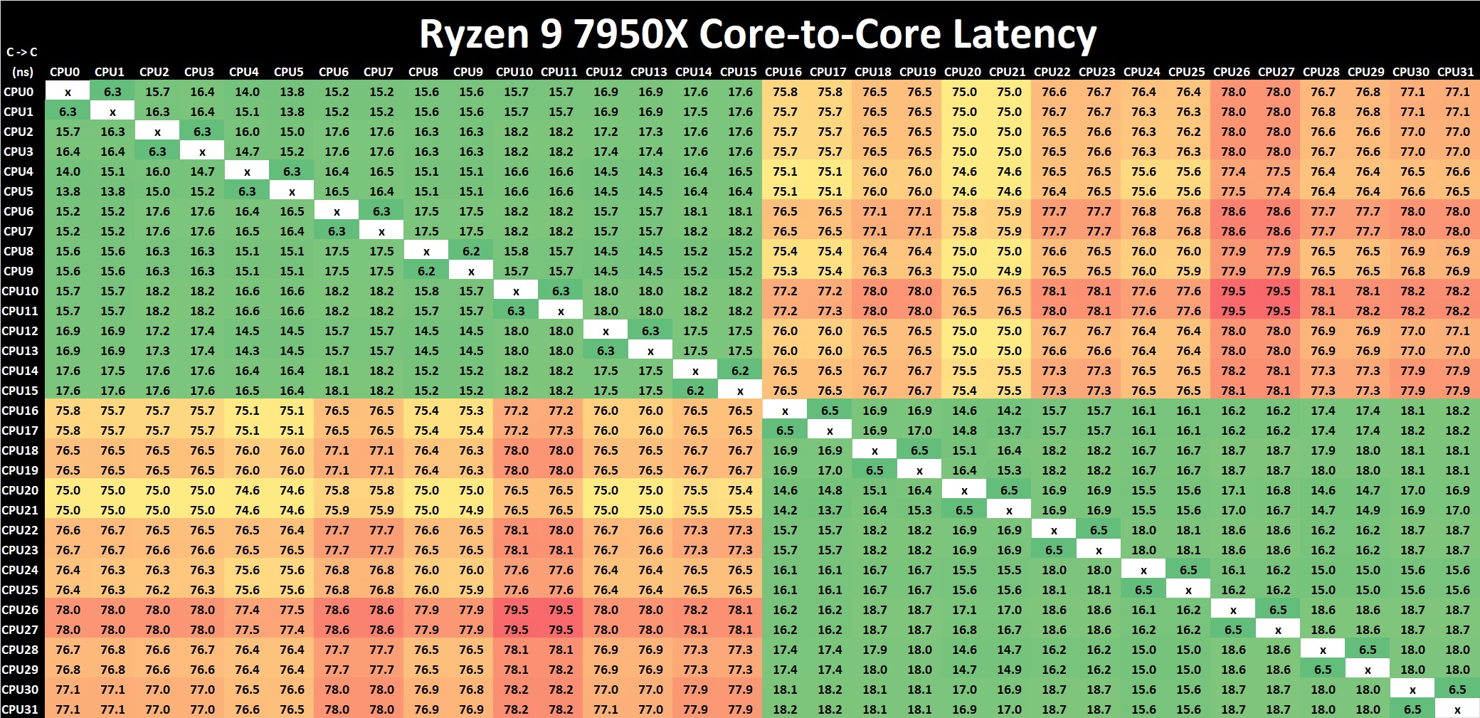
Click to enlarge (lots of cores and threads = lots of core pairings)
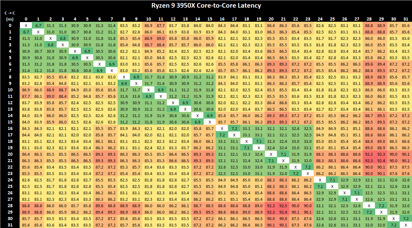
Comparing core to core latencies from Zen 4 (7950X) and Zen 3 (5950X), both are using a two CCX 8-core chiplet design, which is a marked improvement over the four CCX 16-core design featured on the Zen 2 microarchitecture, the Ryzen 9 3950X. The inter-core latencies within the L3 cache range from between 15 ns and 19 ns. The inter-core latencies between different cores within different parts of the CCD show a larger latency penalty of up to 79.5 ns, which is something AMD should work on going forward, but it's an overall improvement in cross CCX latencies compared to Zen 3. Any gain is still a gain.
Even though AMD has opted for a newer and more 'efficient' IOD which is based on TSMC's 6 nm node. It is around the same size physically as the previous AMD IOD on Zen 3 manufactured on GlobalFoundries 12 nm node, but with a much larger transistor count. Within the IOD is the newly integrated RDNA 2 graphics, although this isn't typical iGPU in the sense that an APU is. A lot of the room on the IOD is made up of the DDR5 memory controller or IMC, as well as the chips PCIe 5.0 lanes, and of course, connects to the logic through its primary interconnect named Infinity Fabric. All of these variables play a part on power, latency, and operation.
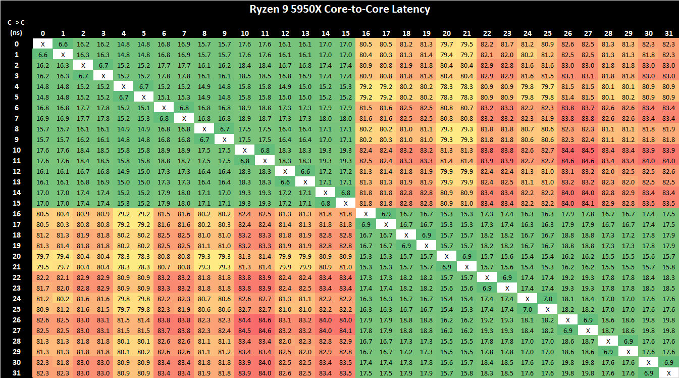
AMD Ryzen 9 5950X Core-to-Core Latency results
It's actually astounding how similar the latency performance of the Ryzen 9 7950X (Zen 4) is when compared directly to the Ryzen 9 5950X (Zen 3), despite being on the new 5 nm TSMC manufacturing process. Even with a change of IOD, but with the same interconnect, the inter-core latencies within the Ryzen 9 7950X are great in terms of cores within the same core complex; latency does degrade when pairing up with a core in another chiplet, but this works and AMD's Ryzen 5000 series proved that the overall penalty performance is negatable.


205 Comments
View All Comments
Oxford Guy - Tuesday, September 27, 2022 - link
This has been posted for years. ReplyBoredInPDX - Tuesday, September 27, 2022 - link
I’m confused. I they 720p tests you write:“All gaming tests here were run using integrated graphics, with a variation of 720p resolutions and at minimum settings.”
Yet all the prior-gen AMD CPUs tested are lacking an IGP. Am I missing something? Reply
Ryan Smith - Friday, September 30, 2022 - link
You are not missing anything; we did not run any iGPU tests. That's a bit of boilerplate text that did not get scrubbed from this article. Thanks for bringing it up! ReplyGigaplex - Wednesday, September 28, 2022 - link
There's some odd results here and the article commentary doesn't seem to touch on it. Why is the 7600X absolutely trounced in Geekbench 4.0 MT? The second slowest CPU (3600XT) more than doubles it. And yet the 7950X wins by a mile in that same test, so it shouldn't be architectural. And in some of the gaming tests, the 7600X wins, and in some it comes dead last. ReplyDribble - Wednesday, September 28, 2022 - link
The processors are particularly cache bound - i.e. it fits in cache it runs very fast, if it doesn't it falls off rapidly. That is often visible in games where it'll run amazingly in some (mostly older) games, but tend to fall off, particularly in the lows, in more complex (mostly newer) games. Replyricebunny - Wednesday, September 28, 2022 - link
The SPEC multithreaded tests are N separate instantiations of the single thread tests. That’s a perfect scenario where there is no dependency or serialization in the workload and tells us very little how the CPUs would perform in a parallel workload application. There are SPEC tests specifically designed to test parallel performance, but I do not see them included in this report. Anandtech, can you comment on this? Replyabufrejoval - Wednesday, September 28, 2022 - link
Emerging dGPUs not supporting PCIe 5.0 is just crippleware!While I can easily see that 16 lanes of PCIe 5.0 won't do much for any game, I can very much see what I'd do with the 8 lanes left over when all dGPU bandwidth requirements can be met with just 8 lanes of PCIe 5.0.
Why can't they just be good PCIe citizens and negotiate to use 16 lanes of PCIe 4.0 on lesser or previous generation boards and optimize lane allocation on higher end PCIe 5.0 systems that can then use bifurcation to add say a 100Gbit NIC, plenty of Thunderbolt 4 or better yet, something CXL?
Actually I'd be really astonished if this wasn't even an artifical cap and that the Nvidia chips may actually be able to do PCIe 5.0.
It's just that they'd much rather have people use NVlink. Reply
TheinsanegamerN - Tuesday, October 4, 2022 - link
Um....dude, 4.0x16 and 5.0x8 have the same bandwidth, and no GPU today can saturate 4.0, not even close. The 300ti OCed manages to saturate.....2.0. 3.0 is a whopping 7% faster.You got awhile man. Reply
abufrejoval - Wednesday, September 28, 2022 - link
It should be interesting to see if AMD is opening the architecture for 3rd parties to exploit the actual potential of the Ryzen 7000 chips.The current mainboard/slot era that dates back to the 1981 IBM-PC (or the Apple ][) really is coming to an end and perhaps few things highlight this as well as a 600 Watt GPU that has a 65 Watt mainboard hanging under it.
We may really need something more S100 or VME, for those old enough to understand that.
Thunderbolt cables handle 4 lanes of PCIe 3.0 today and AFAIK cables are used for much higher lane counts and PCIe revisions within high-end server chassis today, even if perhaps at shorter lengths and with connectors designed for somewhat less (especially less frequent) pluggability.
Their main advantage is vastly reduced issues with mainboard traces and much better use of 3D space to optimize air flow cooling.
Sure those cables aren't cheap, but perhaps the cross-over point for additional PCB layers has been passed. And optical interconnects are waiting in the wings: they will use cables, too.
You stick PCIe 5.0 x4 fixed length cables out from all sides of an AM5 socket and connect those either to high bandwidth devices (e.g. dGPU) or a switch (PCIe 5.0 variant of the current ASMedia), you get tons of flexibility and expandability in a box form factor, that may not resemble an age old PC very much, but deliver tons of performance and expandability in a deskside form factor.
You want to recycle all your nice PCIe 3.0 2TB NVMe drives? Just add a board that puts a PCIe 5.0 20 lane switch between (even PCIe 4.0 might do fine if it's 50% $$$).
And if your dGPU actually needs 8 lanes of PCIe 5.0 to deliver top performance, connect two of those x4 cables to undo a bit of bifurcation!
How those cable connected board would then mount in a chassis and be cooled across a large range of form factors and power ranges is up for lots of great engineers to solve, while dense servers may already provide lots of the design bricks.
Unfortunately all that would require AMD to open up the base initialization code and large parts of the BIOS, which I guess currently has the ASmedia chip(s) pretty much hardwired into it.
And AMD with all their "we don't do artificial market segmentation" publicity in the past, seem to have become far more receptive to its bottom line benefits recently, to allow a free transition from console to PC/workstation and servers of all sizes.
And it would take a high-volume vendor (or AMD itself), a client side Open Compute project or similar to push that form factor the the scale where it becomes economically viable.
It's high time for a PC 2.0 (which isn't a PS/2) to bridge into the CXL universe even on desktops and workstations. Reply
Oxford Guy - Wednesday, September 28, 2022 - link
"The current mainboard/slot era that dates back to the 1981 IBM-PC (or the Apple ][)"Absolutely nothing about the IBM PC was new. The Micral N introduced slots in a microcomputer and the S-100 bus, introduced by the Altair, became the first big standard. Reply