AMD Zen 4 Ryzen 9 7950X and Ryzen 5 7600X Review: Retaking The High-End
by Ryan Smith & Gavin Bonshor on September 26, 2022 9:00 AM ESTZen 4 Execution Pipeline: Familiar Pipes With More Caching
Finally, let’s take a look at the Zen 4 microarchitecture’s execution flow in-depth. As we noted before, AMD is seeing a 13% IPC improvement over Zen 3. So how did they do it?
Throughout the Zen 4 architecture, there is not any single radical change. Zen 4 does make a few notable changes, but the basics of the instruction flow are unchanged, especially on the back-end execution pipelines. Rather, many (if not most) of the IPC improvements in Zen 4 come from improving cache and buffer sizes in some respect.
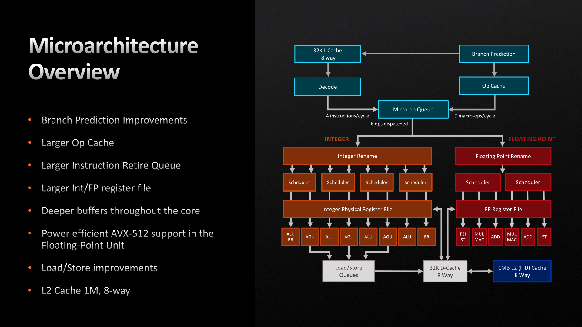
Starting with the front end, AMD has made a few important improvements here. The branch predictor, a common target for improvements given the payoffs of correct predictions, has been further iterated upon for Zen 4. While still predicting 2 branches per cycle (the same as Zen 3), AMD has increased the L1 Branch Target Buffer (BTB) cache size by 50%, to 2 x 1.5k entries. And similarly, the L2 BTB has been increased to 2 x 7k entries (though this is just an ~8% capacity increase). The net result being that the branch predictor’s accuracy is improved by being able to look over a longer history of branch targets.
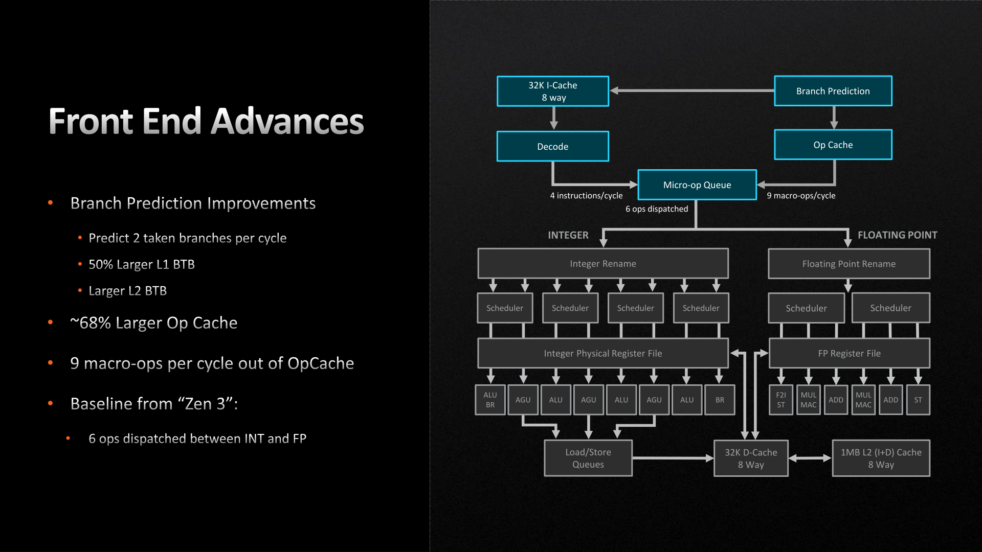
Meanwhile the branch predictor’s op cache has been more significantly improved. The op cache is not only 68% larger than before (now storing 6.75k ops), but it can now spit out up to 9 macro-ops per cycle, up from 6 on Zen 3. So in scenarios where the branch predictor is doing especially well at its job and the micro-op queue can consume additional instructions, it’s possible to get up to 50% more ops out of the op cache. Besides the performance improvement, this has a positive benefit to power efficiency since tapping cached ops requires a lot less power than decoding new ones.
With that said, the output of the micro-op queue itself has not changed. The final stage of the front-end can still only spit out 6 micro-ops per clock, so the improved op cache transfer rate is only particularly useful in scenarios where the micro-op queue would otherwise be running low on ops to dispatch.
Switching to the back-end of the Zen 4 execution pipeline, things are once again relatively unchanged. There are no pipeline or port changes to speak of; Zen 4 still can (only) schedule up to 10 Integer and 6 Floating Point operations per clock. Similarly, the fundamental floating point op latency rates remain unchanged as 3 cycles for FADD and FMUL, and 4 cycles for FMA.
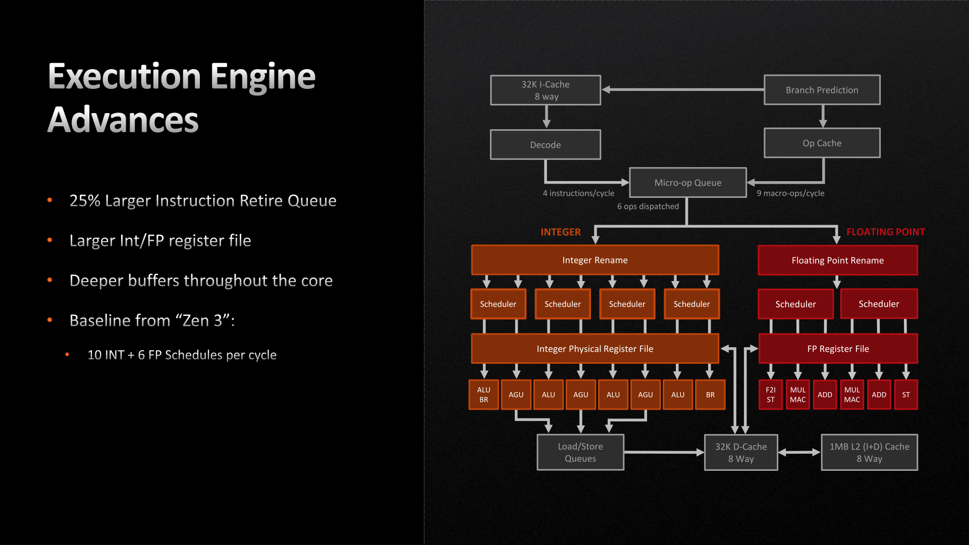
Instead, AMD’s improvements to the back-end of Zen 4 have here too focused on larger caches and buffers. Of note, the retire queue/reorder buffer is 25% larger, and is now 320 instructions deep, giving the CPU a wider window of instructions to look through to extract performance via out-of-order execution. Similarly, the Integer and FP register files have been increased in size by about 20% each, to 224 registers and 192 registers respectively, in order to accommodate the larger number of instructions that are now in flight.
The only other notable change here is AVX-512 support, which we touched upon earlier. AVX execution takes place in AMD’s floating point ports, and as such, those have been beefed up to support the new instructions.
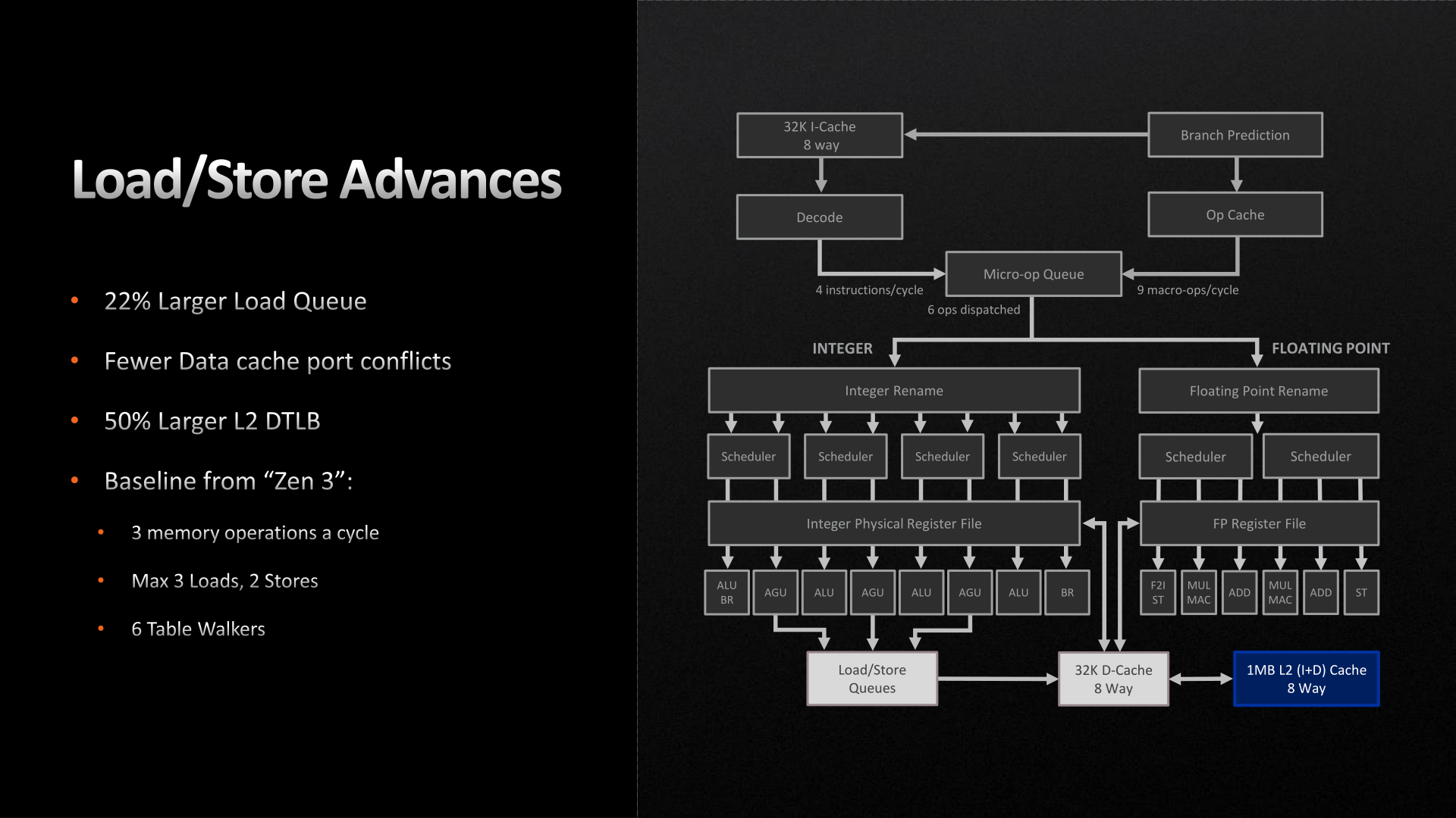
Moving on, the load/store units within each CPU core have also been given a buffer enlargement. The load queue is 22% deeper, now storing 88 loads. And according to AMD, they’ve made some unspecified changes to reduce port conflicts with their L1 data cache. Otherwise the load/store throughput remains unchanged at 3 loads and 2 stores per cycle.
Finally, let’s talk about AMD’s L2 cache. As previously disclosed by the company, the Zen 4 architecture is doubling the size of the L2 cache on each CPU core, taking it from 512KB to a full 1MB. As with AMD’s lower-level buffer improvements, the larger L2 cache is designed to further improve performance/IPC by keeping more relevant data closer to the CPU cores, as opposed to ending up in the L3 cache, or worse, main memory. Beyond that, the L3 cache remains unchanged at 32MB for an 8 core CCX, functioning as a victim cache for each CPU core’s L2 cache.
All told, we aren’t seeing very many major changes in the Zen 4 execution pipeline, and that’s okay. Increasing cache and buffer sizes is another tried and true way to improve the performance of an architecture by keeping an existing design filled and working more often, and that’s what AMD has opted to do for Zen 4. Especially coming in conjunction with the jump from TSMC 7nm to 5nm and the resulting increase in transistor budget, this is good way to put those additional transistors to good use while AMD works on a more significant overhaul to the Zen architecture for Zen 5.


205 Comments
View All Comments
AndrewJacksonZA - Monday, September 26, 2022 - link
I would imagine it's a technically correct way of saying that it's certified for Windows 11. See here about the TPM:www DOT microsoft DOT com/security/blog/2020/11/17/meet-the-microsoft-pluton-processor-the-security-chip-designed-for-the-future-of-windows-pcs/ Reply
socket420 - Monday, September 26, 2022 - link
I'm primarily asking whether or not the Pluton security coprocessor has been incorporated into Raphael/Ryzen 7000 CPUs, and I'm pretty sure that isn't what they were implying - Microsoft *does* have a "secured-core PC" baseline for Win11 they've been pushing lately, but it's currently unclear how Pluton ties into that so I don't think Win11 "certification" has anything to do with it. Pluton wasn't mentioned in AMD's desktop Ryzen 7000 press release last month, I didn't see it in any of the Zen 4 architectural slides they showed off today and AnandTech is the only outlet that's brought it up at all, which is why I'm asking this question in the first place - AMD hasn't been particularly forthcoming about the subject and I feel like they would've mentioned Pluton in a press release if it was actually present in these chips. ReplyRyan Smith - Monday, September 26, 2022 - link
I am not privy to the implementation details. But like other parts of the IOD, Pluton is inherited from the Ryzen 6000 Mobile parts. So it has the same Pluton implementation as those mobile chips.TL;DR: I don't know how they're technically accomplishing it, but yes, Pluton is there and enabled. Reply
socket420 - Tuesday, September 27, 2022 - link
Thanks for the response. Just to clarify, if I reread that section correctly, the Ryzen 7000 I/O die is a new design that had most of the additions from Ryzen 6000 ported over to it, Pluton included. That sounds incredibly damning, but I'm not sure how it's possible to confirm its presence without implementation details. I'm also unsure why AMD would brag about Pluton being present in two different mobile CPU releases from the moment they were announced while seemingly ignoring it in their new and shiny desktop Ryzen lineup up until its release date (are they hoping we won't notice?), but then again, it's been months since Ryzen 6000 was launched and no one's taken a closer look at its Pluton implementation yet, so :/IIRC, Lenovo ships their Ryzen 6000 Thinkpads with Pluton disabled and you have to go into their BIOS to toggle it on or off, so maybe that option showing up on consumer AM5 boards will show us if Pluton's there or not? It'd also be cool if someone asked AMD directly for a response, but Robert Hallock said he "didn't know" if Pluton was in Zen 4 and he coincidentally just left the company, so I have no idea who to reach out to. Reply
Silver5urfer - Tuesday, September 27, 2022 - link
Thanks for your question and this new garbage Pluton cancer is what I did not want to see shame how they added it. ReplyOxford Guy - Tuesday, September 27, 2022 - link
You will own nothing and be owned by everything. You will be happy. ReplyValantar - Monday, September 26, 2022 - link
Could you please run your per-core power draw tests for these chips like you did for Zen3? Replytakling1986 - Monday, September 26, 2022 - link
I think this review is "streets ahead". ReplyIBM760XL - Monday, September 26, 2022 - link
All right, since they aren't read yet, I'll ask... is it easy to set a lower TDP limit, and could you examine power efficiency when the TDP is the same as it was for Ryzen 5000?Looking at the numbers Tom's Hardware posted, the 7950X uses about 80W more at load than the 5950X. With AMD's own slides touting the efficiency improvements being greater at lower TDPs, what I'd really like is to have an octo-core at 65W like the 5700, or perhaps a 12/16 core at 105W like the 5900/5950.
Though I'm very likely to wait until B650 drops before making a decision, so there's plenty of time for an answer to that question to arrive. Reply
abufrejoval - Wednesday, September 28, 2022 - link
I can only guess that it should be trival to do via RyzenMaster, just in case it's not supported in the BIOS. And of course I'd demand CLI tools for both Linux and Windows.I cannot imagine that with a max TDP of 140 Watts a 7950X won't still be faster than a 5950X, even if it won't be quite as fast as if you let it drain the bottle at full hilt. The typical CMOS knee will still be there, only moved forward a bit and with a lot more of a "hot leg" showing towards the top.
But gains per clock and Watt will be terrible the higher you go on the "hot leg" by nature of silicon physics and any sensible person will just use a "lesser cooler" to avoid that nonsense. Reply