Intel 12th Gen Core Alder Lake for Desktops: Top SKUs Only, Coming November 4th
by Dr. Ian Cutress on October 27, 2021 12:00 PM EST- Posted in
- CPUs
- Intel
- DDR4
- DDR5
- PCIe 5.0
- Alder Lake
- Intel 7
- 12th Gen Core
- Z690
Package Improvements
As we move to smaller process nodes, the thermal density of high-performance silicon becomes more of an issue, and so all the processor companies put resources into their mechanical design teams to come up with a solution for the best thermal performance but also comes in line with costs. For example, we’ve seen Intel over the years transition from a soldered down heatspreader, to liquid metal, to basic thermal paste (because saving 0.1 cents means a lot across 70m CPUs), and then all the way back again when customers started demanding it.
However, in that time, we’ve pretty much kept the same socket design for mainstream processors. There hasn’t been much emphasis on changing the design itself for thermomechanical improvements in order to retain reuse and compatibility. There have been some minor changes here and there, such as substrate thinning, but nothing that substantial. The move to a new socket for Alder Lake now gives Intel that opportunity.
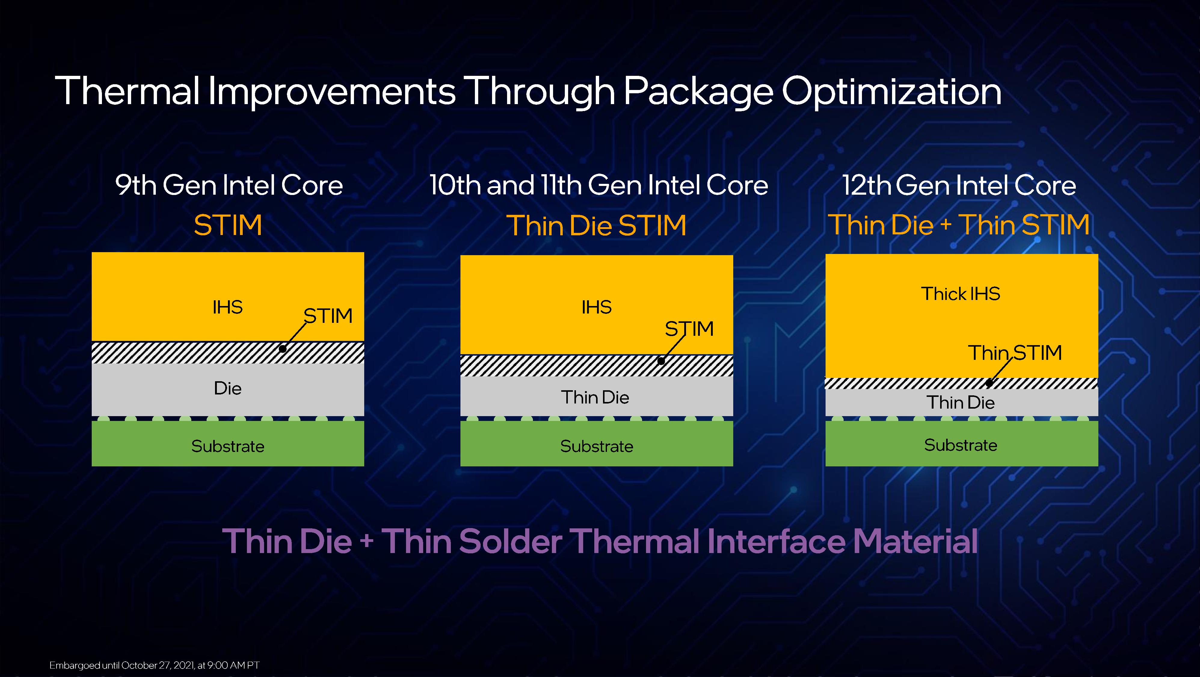
For Alder Lake, Intel is using an optimized packaging process to reduce the amount of soldered thermal material used in the processors. Combining that with a thinner die, and Intel is having to increase the thickness of the heatspreader to maintain the required z-height for the platform. The idea here is that the limiting factor in the cooling solution is any time we have a thermal interface, from one material to another – in this case, die to solder, and solder to heatspreader. Solder is the weak point here, so if the heatspreader gets thicker to meet the die, then less solder is needed.
Ultimately direct-die liquid cooling would be the boon here, but Intel has to come up with a solution that fits millions of processors. We have seen Intel offer different packaging solutions based on the SKU itself, so it will be interesting if the mid-range still get the Thin Die + Thin STIM treatment, or if they’ll go back to the cheap thermal paste.
Overclocking: We Have Headroom
It wouldn’t be too much of a leap to say that for most users, the only useful overclocking they might want to look at is enabling XMP on their memory. Modern processors these days are so close to their actual voltage and thermal limits out of the box these days that even if there was 200-300 MHz to gain, especially for the top Core i9 parts, it wouldn’t be worth the +100W it produces. I’m also getting to an age now where I prefer a good stable system, rather than eking out every frame, but having lived in the competitive OC scene for a while, I understand the drive that a lot of those users have to go above and beyond. To that end, Intel is introducing a few new features, and reviving some old ones, for Alder Lake.
Alder Lake also complicates things a bit with the P-core and E-core design.
To start, all the cores on the K/KF parts can be overclocked. The P-cores can be overclocked individually, whereas the E-cores are in groups of four. All the E-cores can be disabled, but at least one P-core needs to be enabled for the system to work (this has interesting consequences for Intel’s design). All cores can have additional AVX offsets, per-core ratio and voltage controls, and the ring/uncore ratios can also be adjusted. Memory also has the bells and whistles mentioned on a previous page. Those with integrated graphics can also be adjusted.
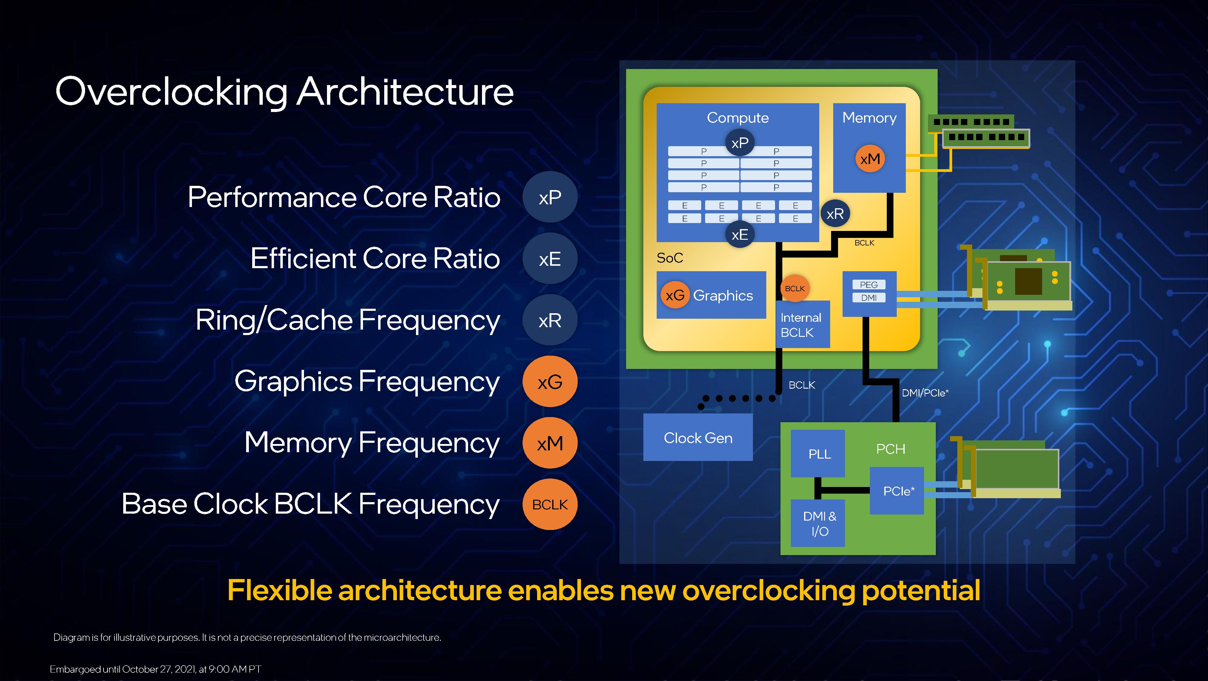
What Alder Lake brings back to the table is BCLK overclocking. For the last decade or so, most overclocking is done with the CPU multiplier, and before that it was BCLK or FSB. Intel is now saying that BCLK overclocking has returned, and this is partly due to motherboard customizations in the clock generator. Every Alder Lake CPU has an internal BCLK/clock generator it can use, however motherboard vendors can also apply an external clock generator. Intel expects only the lowest-end motherboards will not have an external generator.
The use of two generators allows the user to overclock the PCIe bus using the external generator, while maintaining a regular BCLK on other parts of the system with the internal clock. The system can also apply voltage in an adaptive way based on the overclock, with additional PLL overrides.
On top of this, Intel is integrating more user-accessible telemetry for its cores, particularly the E-cores, and real-time frequency analysis. On top of this, users can adjust the memory frequency in the operating system, rather than having to reboot – this is an extension of the memory turbo functionality previously mentioned.
For regular users, Intel is also offering a one-click immediate overclock feature. On launch, the Core i9 will be supported and overclock the P-cores +100 MHz and the E-cores +300 MHz immediately. It sounds like Intel is confident that all CPUs will be able to do this, but they want it to be user selectable. Beyond that, I confirmed the tool does still void the warranty. Intel’s VP dismissed it as an issue, citing that the recent overclocker warranty program they canned had such a low pickup, it wasn’t worth continuing. I’d say that the two things are mutually exclusive, but that’s up to Intel.


395 Comments
View All Comments
Qasar - Friday, October 29, 2021 - link
yea, according to leaks maybe. remember how the 1100 series went ?untill reviews are out, its all speculation
Josh128 - Wednesday, October 27, 2021 - link
Intel's only chance to beat Zen 4 is if they get their "Intel 4" 7nm process going. If they have to stay on "Intel 7" 10nm, thats not going to cut it against TSMC 5 /5 +.regsEx - Wednesday, October 27, 2021 - link
Why calling Intel 4 as 7 nm process and Intel 7 as 10 nm process, but not mentioning TSMC N5 as 9 nm process?Spunjji - Thursday, October 28, 2021 - link
Two reasons:N5 was never renamed
"Intel 7" is still not equivalent to TSMC N7 on either density or power characteristics. Who knows how "Intel 4" will compare to N5 - if it's a similar relationship to Intel 7 and TSMC N7, then it should be called Intel 6.
shady28 - Thursday, October 28, 2021 - link
Intel 7 aka 10ESF is about the same density as TSMC N7FF+. It is reportedly 100.76 MT/mm2 vs TSMC N7FF of 96.5 MT/mm2. That's easy to validate doing your own research. This doesn't mean that Intel is not behind TSMC 5nm, but it is no longer behind their 7nm.https://semiwiki.com/semiconductor-manufacturers/s...
https://fuse.wikichip.org/news/1371/a-look-at-inte...
Spunjji - Friday, October 29, 2021 - link
@shady28 - those are the official figures, sure. It's a little more difficult to validate those, but luckily I have done my own research!In reality neither Intel nor TSMC can hit their claimed densities in actual chips, for a variety of reasons. The best information we have suggests that AMD have managed 62.8MTr/mm² on TSMC N7 with Renoir (Cezanne is an oddball because it has blank die space). Meanwhile Intel's competing chip - Ice Lake - clocked in at 53.2MTr/mm² on 10nm+. It's not a vast difference, but it's a difference all the same.
What we don't know is how the 10 SF and 10 ESF (now Intel 7) process changes have affected density. There's circumstantial evidence to suggest that 10 SF involved a relaxation of density, but we don't really know because Intel have been extremely tight-lipped about it.
Zoolook - Saturday, October 30, 2021 - link
In efficiency they sure are i.e performance/watt on the CPU's produced they are way behind.melgross - Friday, October 29, 2021 - link
It’s really more like a 7nm Intel process.Samus - Friday, October 29, 2021 - link
What's important of note here is AMD has had a fantastic run, effectively beating Intel in most categories for the last few years. Now Intel may be caught up and they are neck and neck.But this wouldn't have happened unless Intel had a fire under their ass.
melgross - Friday, October 29, 2021 - link
The way AMD had a fire under their ass