Arm Announces Mobile Armv9 CPU Microarchitectures: Cortex-X2, Cortex-A710 & Cortex-A510
by Andrei Frumusanu on May 25, 2021 9:00 AM EST- Posted in
- SoCs
- CPUs
- Arm
- Smartphones
- Mobile
- Cortex
- ARMv9
- Cortex-X2
- Cortex-A710
- Cortex-A510
New DSU-110 L3 & Cluster: Massively More Bandwidth
Alongside the new CPU microarchitectures, Arm today is also announcing a new L3 design in the form of the new DSU-110. The “DynamIQ Shared Unit” had been the company’s go-to cluster and “core complex” block ever since it was introduced in 2017 with the Cortex-A75 and Cortex-A55. While we’ve seen small iterative improvements, today’s DSU-110 marks a major change in how the DSU operates and how it promises to scale up in cache size and bandwidth.
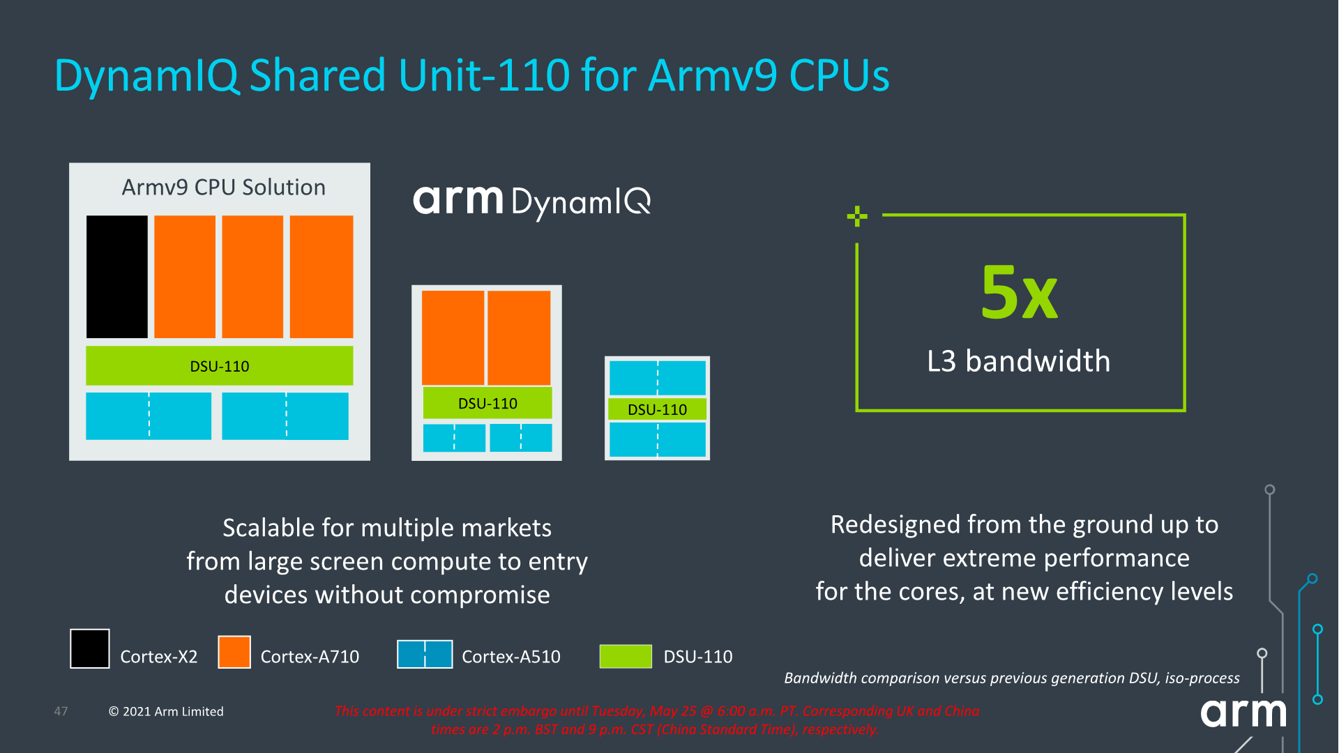
The new DSU-110 is a ground-up redesign with an emphasis on more bandwidth and more power efficiency. It continues to be the core building block for all of Arm’s mobile and lower tier market segments.
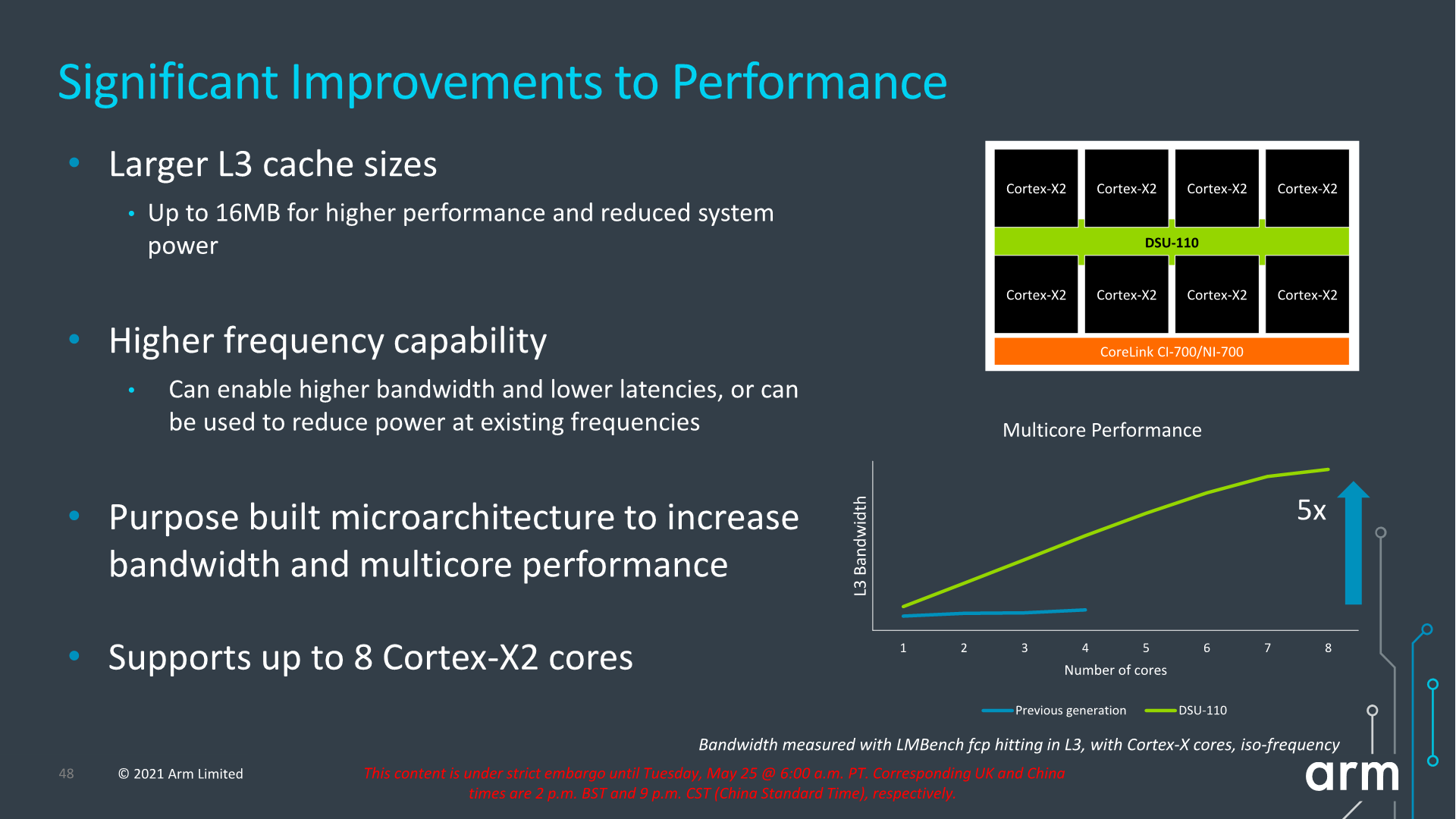
A key metric is of course the increase of L3 cache configuration which will now go up to 16MB this generation. This is of course the high-end of the spectrum and generally we shouldn’t expect such a configuration in a mobile SoC soon, but Arm has had several slides depicting larger form-factor implementations using such a larger design housing up to 8 Cortex-X2 cores. This is undoubtedly extremely interesting for a higher-performance laptop use-case.
The bandwidth increase of the new design is also significant, and applies from single-thread to multi-threaded scenarios. The new DSU-110 promises aggregate bandwidth increases of up to 5x compared to the contemporary design. More interesting is the fact that it also significantly boosts single-core bandwidth, and Arm here actually notes that the new DSU can actually support more bandwidth than what’s actually capable of the new core microarchitectures for the time being.
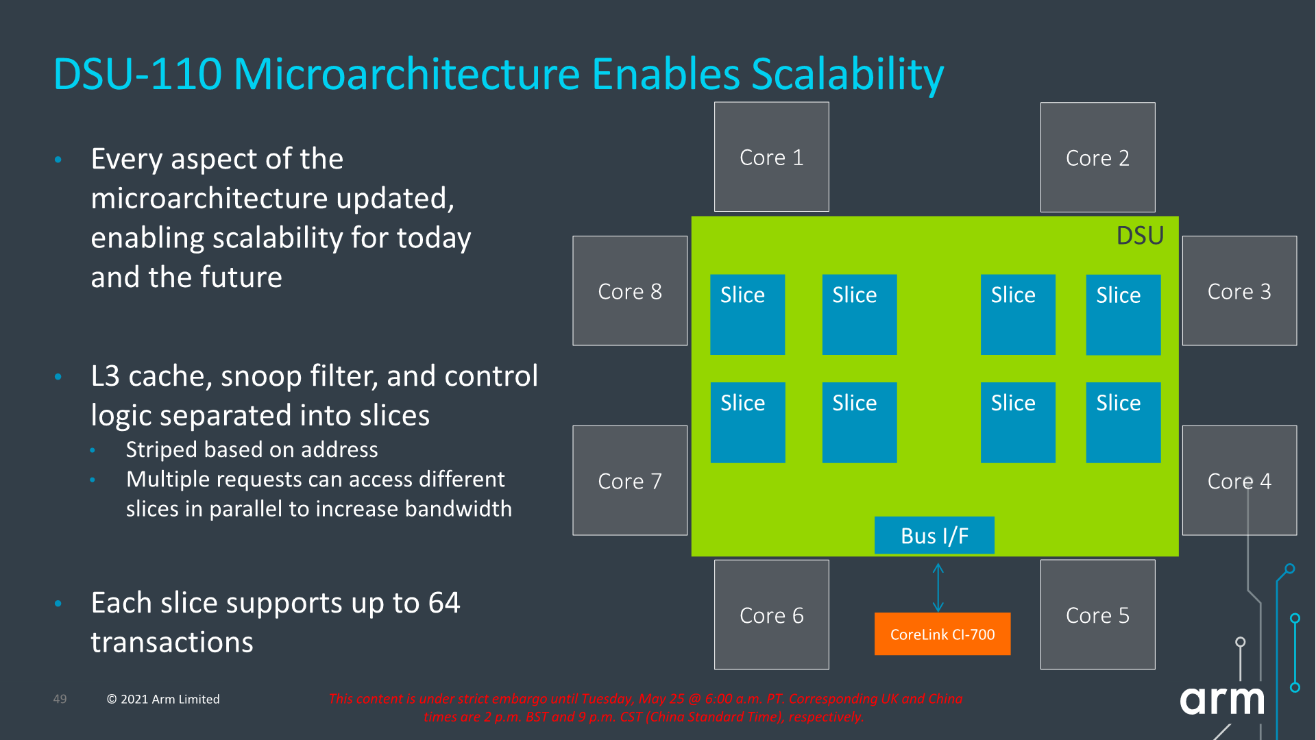
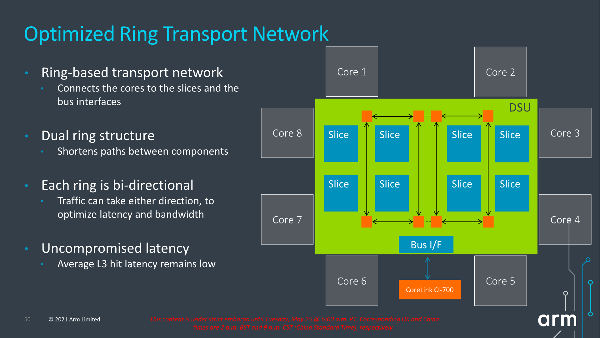
Arm never really disclosed the internal topology of the previous generation DSU, but remarks that with the DSU-110 the company has shifted over to a bi-directional dual-ring transport topology, each with four ring-stops, and now supporting up to 8 cache slices. The dual-ring structure is used to reduce the latencies and hops between ring-stops and in shorten the paths between the cache slices and cores. Arm notes that they’ve tried to retain the same lower access latencies as on the current generation DSU (cache size increases aside), so we should be seeing very similar average latencies between the two generations.
Parallel access increases for bandwidth as well as more outstanding transactions seem to have been also very important in order to improve performance, which seems very exciting for upcoming SoC designs, but also puts into more question the previously presented CPU IPC improvements and exactly how much the new DSU-110 contributes to those numbers.
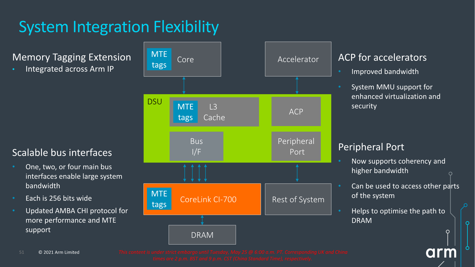
Architecturally, one important change to the capabilities of the DSU-110 is support for MTE tags, a upcoming security and debugging feature promising to greatly help with memory safety issues.
The new DSU can scale up to 4x AMBA CHI ports, meaning we’ll have up to 1024-bit total bi-directional bandwidth to the system memory. With a theoretical DSU clock of around 2GHz this would enable bandwidth of up to 256GB/s reads or writes, or double that when combined, plenty enough to be able to saturate also eventual high-end laptop configurations.

In terms of power efficiency, the new DSU offers more options for low-power operation when in idle situations, implementing partial L3 power-down, able to reduce leakage power of up to 75% compared to the current DSU.
In general idle situations but still having the full L3 powered on, the new design promises up to 25% reduction in leakage power all whilst offering 2x the bandwidth capabilities.
It’s important to note that we’re talking about leakage power here- active dynamic power is expected to generally scale linearly with the bandwidth increase of the new design, meaning 5x the bandwidth would also cost 5x the power. This would be an important factor to note into system power and in general the expected power behaviour of the next-gen SoCs when they’re put under heavy memory workloads.
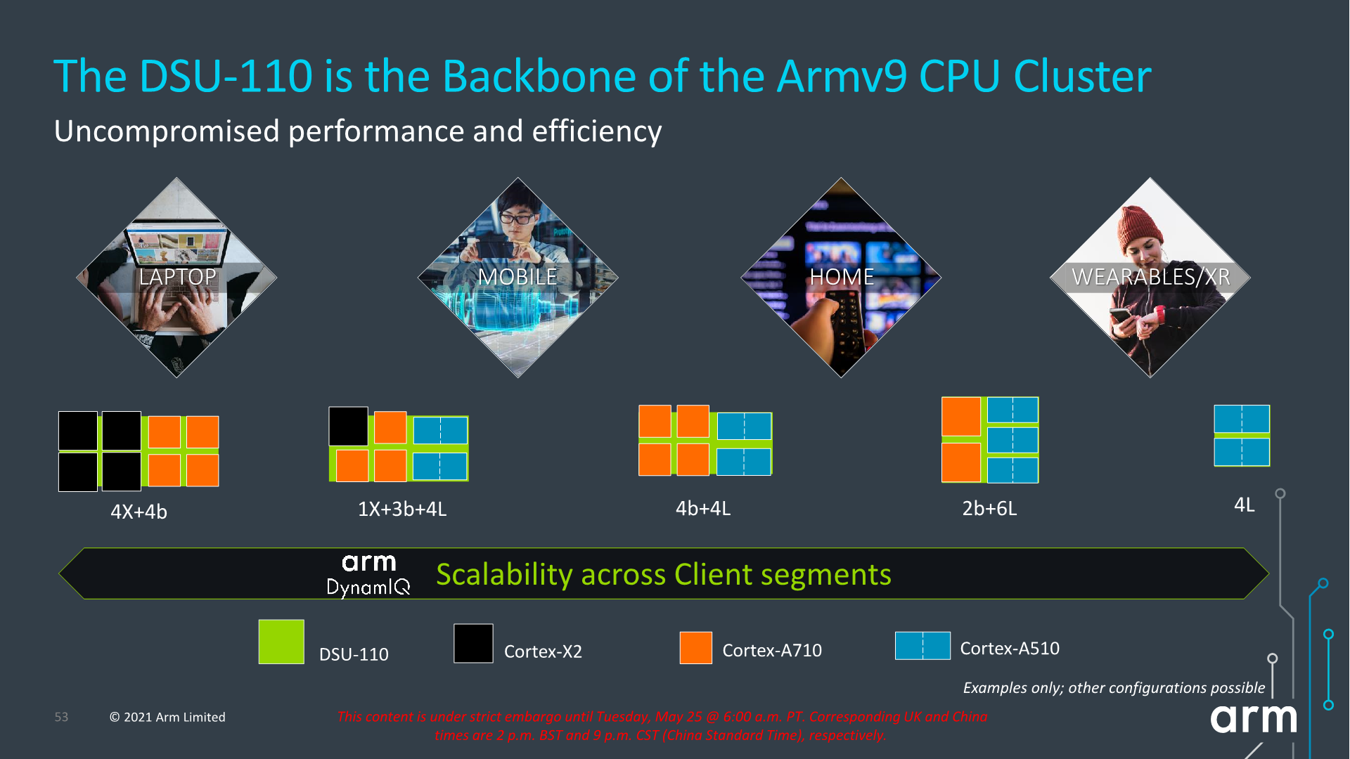
Arm describes the DSU-110 as the backbone of the Armv9 cluster and that seemingly seems to be an apt description. The new bandwidth capabilities are sure to help out both with single-threaded, but also with multi-threaded performance of upcoming SoCs. Generally, the new 16MB L3 capability, while it’s possible somebody might do a high-end laptop SoC configuration, isn’t as exciting as the now finally expected move to a new 8MB L3 on mobile SoCs, hopefully also enabling higher power efficiency and more battery life for devices.


181 Comments
View All Comments
WorBlux - Thursday, May 27, 2021 - link
These micro-ops are greatly exaggerated. For instance Gracemont CPU's don't have any. And 4 of the 5 decoders on intel are simple, meaning they only drop one micro-op per instruction.Having to deal with a variable length instruction is still a bitch on the front end.
mode_13h - Saturday, May 29, 2021 - link
> Gracemont CPU's don't have any.I think you meant to say they don't have micro-op *caches*.
Tomatotech - Tuesday, May 25, 2021 - link
They’re correct. x86 cores have been RISC internally since the Pentium era. They’re black boxes that take CISC instructions, then internally these instructions are converted to RISC for the microprocessors.See the Development section of this wiki article for the Pentium. Later chips expanded and further developed the internal RISC parts after the success of the Pentium. Sorry to shatter your illusions.
https://en.wikipedia.org/wiki/P5_(microarchitectur...
Wilco1 - Tuesday, May 25, 2021 - link
RISC/CISC is only ever about the ISA, never about implementation. Even the very first 8086 uses simpler micro-ops internally in its microcode, but that doesn't make it any more RISC than modern implementations.Another common misconception that changing the decoder is all that is required to change ISAs. This is also incorrect since the internals are very different between ISAs.
Thala - Tuesday, May 25, 2021 - link
Precisely. x86 will never escape from the problem:- having variable length instructions
- having less architectural registers
- having TSO memory model
And no internal RISC-like microarchitecture will help with above issues.
GeoffreyA - Wednesday, May 26, 2021 - link
"having variable length instructions"The main bottleneck of x86 and the part where ARM has the upper hand. Still, it's not impossible that some genius at AMD or Intel could crack the variable-length handicap once and for all. The micro-op cache did much. Something else is still missing.
mode_13h - Wednesday, May 26, 2021 - link
> Still, it's not impossible that some genius at AMD or> Intel could crack the variable-length handicap once and for all.
The only solution I see to that is basically letting the uop cache spill to RAM, so the decoder works more like a JIT translation engine.
And that only solves *one* of x86's key detriments.
GeoffreyA - Thursday, May 27, 2021 - link
That's a possibility but more work on the OS side. In that case, it might be better to switch to a new, fixed-length ISA altogether.If there were some way to index instruction start/end before reaching the decoder. Perhaps the compiler could help but that might break compatibility.
mode_13h - Saturday, May 29, 2021 - link
> That's a possibility but more work on the OS side.Yes. The era of "free" CPU performance improvements is coming to an end.
> In that case, it might be better to switch to a new, fixed-length ISA altogether.
Well, it's one thing Intel or AMD could do to eke a little more life out of x86-64. I think it's actually not a lot to ask from operating systems.
> If there were some way to index instruction start/end before reaching the decoder.
Perhaps the L1 instruction cache could do some preliminary analysis, during fills. They could add a couple extra bits per byte, to hold information subsequently useful to the decoder.
Or, maybe the decoder could just write back some info to help itself, if it needs to re-decode those same instructions after the corresponding micro-ops have been evicted from the micro-op cache.
GeoffreyA - Monday, May 31, 2021 - link
"Perhaps the L1 instruction cache could do some preliminary analysis"Interestingly, some CPUs did mark the instruction boundaries in the cache. Possibly the same principle. If I remember right, the Pentium MMX and some of the Atoms; and on AMD's side, K7 all the way to Bulldozer.