Arm Announces Mobile Armv9 CPU Microarchitectures: Cortex-X2, Cortex-A710 & Cortex-A510
by Andrei Frumusanu on May 25, 2021 9:00 AM EST- Posted in
- SoCs
- CPUs
- Arm
- Smartphones
- Mobile
- Cortex
- ARMv9
- Cortex-X2
- Cortex-A710
- Cortex-A510
New DSU-110 L3 & Cluster: Massively More Bandwidth
Alongside the new CPU microarchitectures, Arm today is also announcing a new L3 design in the form of the new DSU-110. The “DynamIQ Shared Unit” had been the company’s go-to cluster and “core complex” block ever since it was introduced in 2017 with the Cortex-A75 and Cortex-A55. While we’ve seen small iterative improvements, today’s DSU-110 marks a major change in how the DSU operates and how it promises to scale up in cache size and bandwidth.
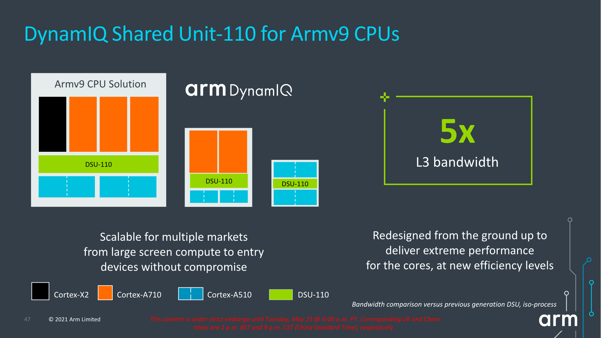
The new DSU-110 is a ground-up redesign with an emphasis on more bandwidth and more power efficiency. It continues to be the core building block for all of Arm’s mobile and lower tier market segments.
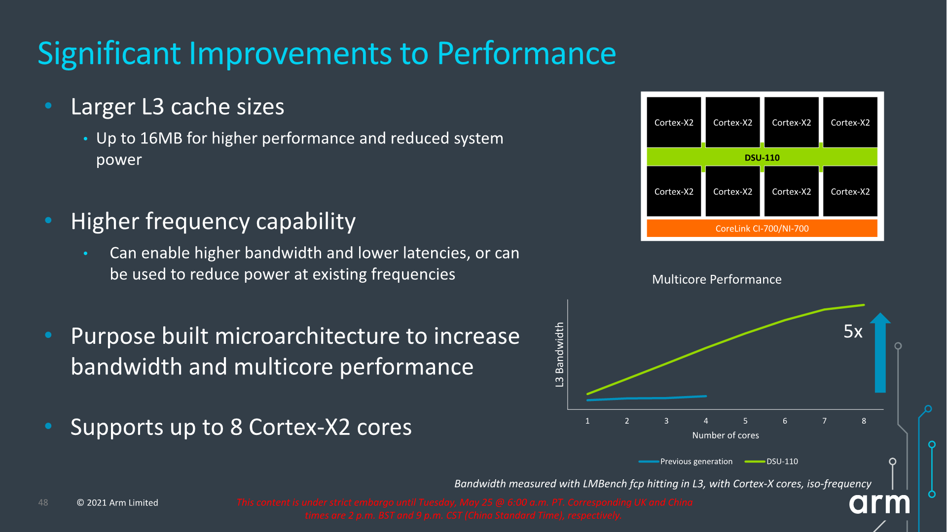
A key metric is of course the increase of L3 cache configuration which will now go up to 16MB this generation. This is of course the high-end of the spectrum and generally we shouldn’t expect such a configuration in a mobile SoC soon, but Arm has had several slides depicting larger form-factor implementations using such a larger design housing up to 8 Cortex-X2 cores. This is undoubtedly extremely interesting for a higher-performance laptop use-case.
The bandwidth increase of the new design is also significant, and applies from single-thread to multi-threaded scenarios. The new DSU-110 promises aggregate bandwidth increases of up to 5x compared to the contemporary design. More interesting is the fact that it also significantly boosts single-core bandwidth, and Arm here actually notes that the new DSU can actually support more bandwidth than what’s actually capable of the new core microarchitectures for the time being.
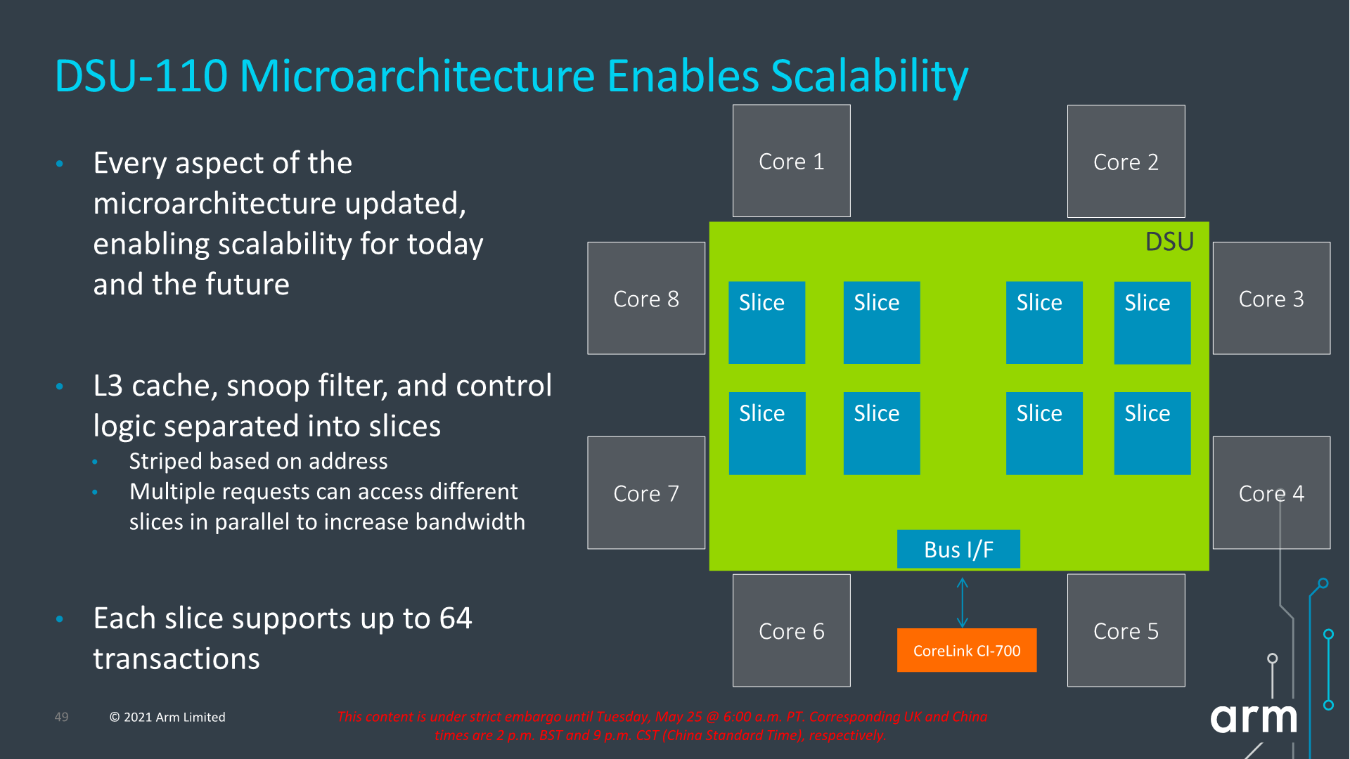
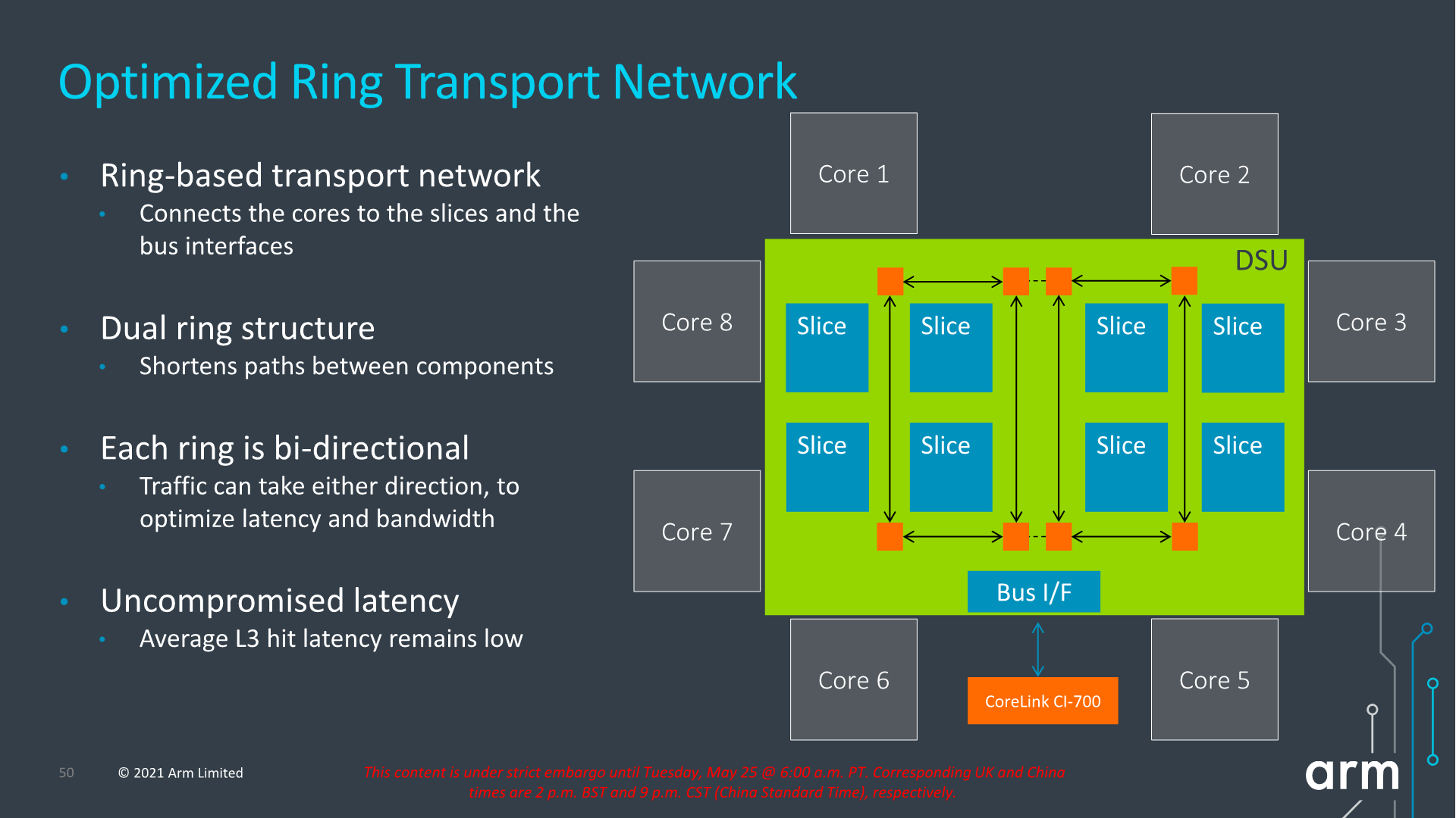
Arm never really disclosed the internal topology of the previous generation DSU, but remarks that with the DSU-110 the company has shifted over to a bi-directional dual-ring transport topology, each with four ring-stops, and now supporting up to 8 cache slices. The dual-ring structure is used to reduce the latencies and hops between ring-stops and in shorten the paths between the cache slices and cores. Arm notes that they’ve tried to retain the same lower access latencies as on the current generation DSU (cache size increases aside), so we should be seeing very similar average latencies between the two generations.
Parallel access increases for bandwidth as well as more outstanding transactions seem to have been also very important in order to improve performance, which seems very exciting for upcoming SoC designs, but also puts into more question the previously presented CPU IPC improvements and exactly how much the new DSU-110 contributes to those numbers.
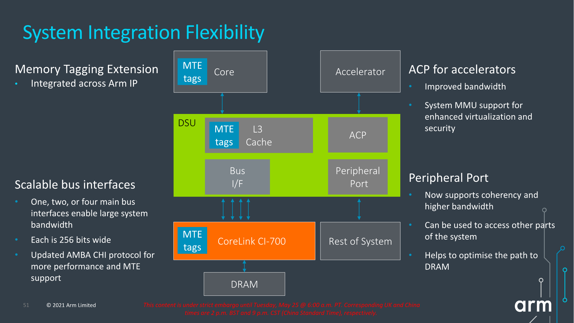
Architecturally, one important change to the capabilities of the DSU-110 is support for MTE tags, a upcoming security and debugging feature promising to greatly help with memory safety issues.
The new DSU can scale up to 4x AMBA CHI ports, meaning we’ll have up to 1024-bit total bi-directional bandwidth to the system memory. With a theoretical DSU clock of around 2GHz this would enable bandwidth of up to 256GB/s reads or writes, or double that when combined, plenty enough to be able to saturate also eventual high-end laptop configurations.

In terms of power efficiency, the new DSU offers more options for low-power operation when in idle situations, implementing partial L3 power-down, able to reduce leakage power of up to 75% compared to the current DSU.
In general idle situations but still having the full L3 powered on, the new design promises up to 25% reduction in leakage power all whilst offering 2x the bandwidth capabilities.
It’s important to note that we’re talking about leakage power here- active dynamic power is expected to generally scale linearly with the bandwidth increase of the new design, meaning 5x the bandwidth would also cost 5x the power. This would be an important factor to note into system power and in general the expected power behaviour of the next-gen SoCs when they’re put under heavy memory workloads.
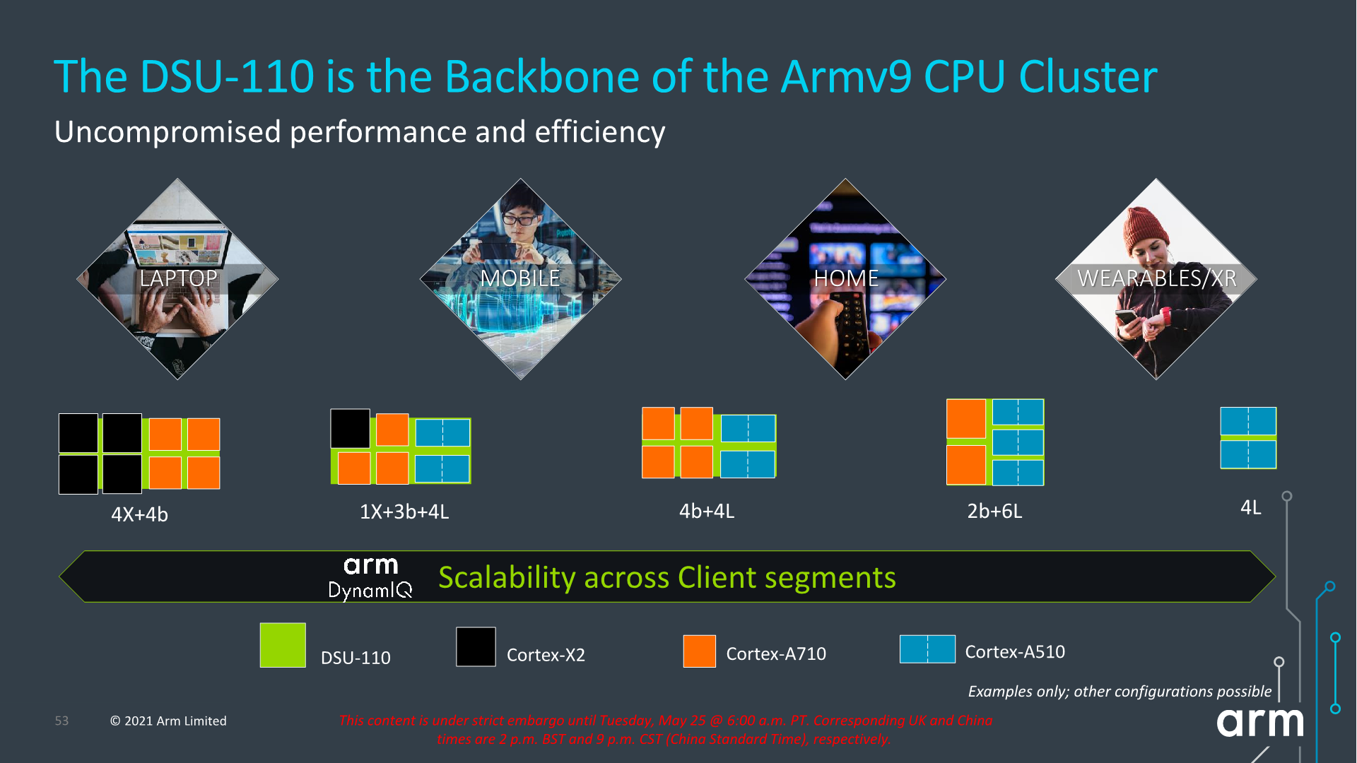
Arm describes the DSU-110 as the backbone of the Armv9 cluster and that seemingly seems to be an apt description. The new bandwidth capabilities are sure to help out both with single-threaded, but also with multi-threaded performance of upcoming SoCs. Generally, the new 16MB L3 capability, while it’s possible somebody might do a high-end laptop SoC configuration, isn’t as exciting as the now finally expected move to a new 8MB L3 on mobile SoCs, hopefully also enabling higher power efficiency and more battery life for devices.


181 Comments
View All Comments
Thala - Tuesday, May 25, 2021 - link
You compare only peak performance. ARM has demonstrated that SVE2 can have big advantages over NEON, in particular for computational kernel, which does not parallelize well for NEON.WorBlux - Thursday, May 27, 2021 - link
>If they are sticking with in-order, I hoped the A510 could’ve done something more over four years.In order is hard. The A55 was pretty cool in allowing certain instruction dependencies to be issued together. The traditional way to get more IPC out of in-order is VLIW, but would require an ABI break or at least a special sort of compiler optimization and quasi-long-words that in the end wouldn't do any better than the A55/A510 on legacy and non-optimized code.
mode_13h - Tuesday, May 25, 2021 - link
x86 is indeed on the way out, but your analysis is too facile.SarahKerrigan - Tuesday, May 25, 2021 - link
Essentially agreed.yeeeeman - Tuesday, May 25, 2021 - link
x86 maybe dead if you don't understand how and why things stand like they do.First of all, Apple is in a very very special situation where they control everything. Hardware, software, product. Plus they use the best process there is at the moment. All of this, contributes to their results. Which are very good, but they stem from what I told you.
Now, a better picture of what ARM is actually capable of in ... real life is the snapdragon 8cx, which for all intents and purposes is still alive only because qualcomm has a ton of money and can throw it away for projects that don't really sell.
Apple is using just ARM ISA. If Apple has great performance and great efficiency, it doesn't mean automatically that ARM and the companies that work with them will also reach that point. The truth is, Apple has put a LOT of money and R&D and got the best talents there are to get where they are today. Their cores are not exactly suited for the plethora of android devices that range from 50 bucks to 2000+.
Now, regarding x86, if you compare amd's zen 3 with m1, you'll see that they are not that far off, in perf and in efficiency. And AMD is using 7nm, not 5nm! Also, nowdays, all the cpus are risc inside, so x86 cpus are very similar inside to arm cpus, with the addition of the extra decoding and micro ops.
x86 main weakness is also its greatest advantage. Backwards compatibility is very important and needs to stay. ARM cpus lose compatibility totally once in a while, which is not something that will work in the long run.
Also, don't forget that Intel hasn't introduced anything major since 2015! Ice Lake/Tigerlake are just a bump in execution units over skylake, which on its own brings 20% better IPC. But Intel has stayed still for so many years, that is why ARM has got the chance to close the gap.
SarahKerrigan - Tuesday, May 25, 2021 - link
What? SNC is not merely a bump in execution units from SKL at all. It's a new, wider, more aggressive uarch across the board. SNC is a larger change than SKL itself was, and not by a small margin.boredsysadmin - Tuesday, May 25, 2021 - link
@yeeeeman - "Also, nowdays, all the cpus are risc inside, so x86 cpus are very similar inside to arm cpus, with the addition of the extra decoding and micro ops."Excuse, where did you get this BS? Only Arm, Risk-V, MIPS, and PowerPC are using RISC. x86 from both Intel and AMD are very much still CISC. So, no they aren't very similar in any share and form.
Drumsticks - Tuesday, May 25, 2021 - link
All x86 CPUs crack CISC macro instructions into smaller RISC like operations. The actual execution of the CPU operates on these smaller micro ops. Beyond the initial decode/cracking stage, it's pretty much a RISC operation.They are CISC from an architectural perspective, but they've been RISC in execution for some time.
vvid - Tuesday, May 25, 2021 - link
>> All x86 CPUs crack CISC macro instructions into smaller RISC like operations.RISC-like is not RISC. It is like saying that a woman with pear-like figure shape is actually a pear.
x86 uops are pretty much corresponding to CISC ISA now.
>> but they've been RISC in execution for some time
RISC-like.
mode_13h - Wednesday, May 26, 2021 - link
> they've been RISC in execution for some time.And sadly, Internet Oversimplification Syndrome claims another victim.