Arm Announces Mobile Armv9 CPU Microarchitectures: Cortex-X2, Cortex-A710 & Cortex-A510
by Andrei Frumusanu on May 25, 2021 9:00 AM EST- Posted in
- SoCs
- CPUs
- Arm
- Smartphones
- Mobile
- Cortex
- ARMv9
- Cortex-X2
- Cortex-A710
- Cortex-A510
A new CI-700 Coherent Interconnect & NI-700 NoC For SoCs
Finally, the last new announcement of the day is a new interconnect and network-on-chip generation. The last time Arm had announced a mobile/client interconnect was back in in 2015 with the CCI-550. The reason for the large gap between IPs, in Arm’s own words, is that ever since Arm’s introduction of the DSU in its CPU complexes, there really hasn’t been any need for a cache coherent interconnect in the market. While that’s eyebrow-raising from a GPU perspective, it makes perfect sense from a CPU perspective, as coherency between CPU cores was the primary driver for such interconnects until then.
With the advent of new more complex computing platforms, such as NPUs, accelerators, and hopeful more use of GPUs in cache-coherent fashions, Arm saw a need gap in its portfolio and decided to update its client-side interconnect IP.
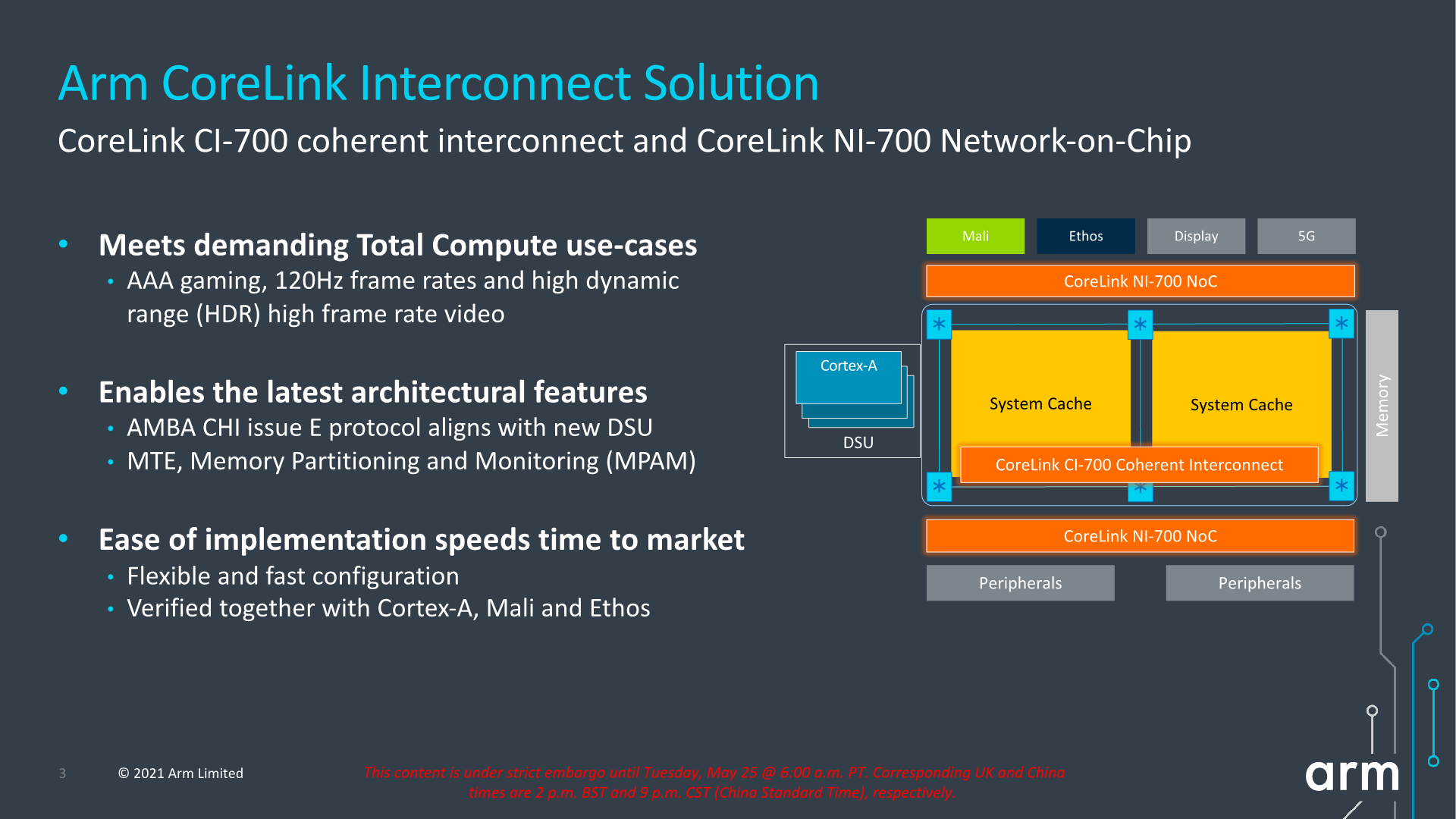
The new CI-700 is a mobile and client optimised variant of Arm’s infrastructure CMN mesh network, implementing important new interoperability with the new IP announced today, such as the new DSU or CPU cores.
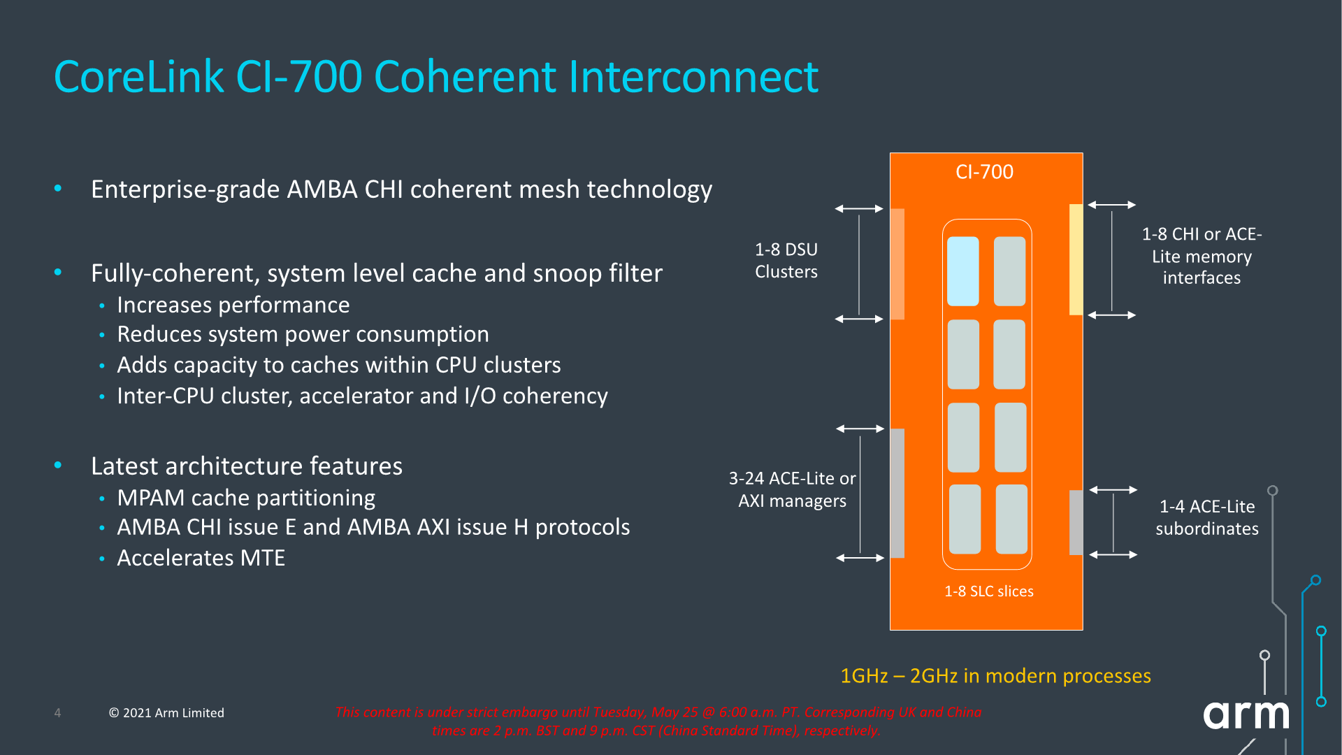
The new mesh interconnect scales up from 1 to 8 DSU clusters, and supports up to 8 memory controllers, and also introduces innovations such as a system level cache.
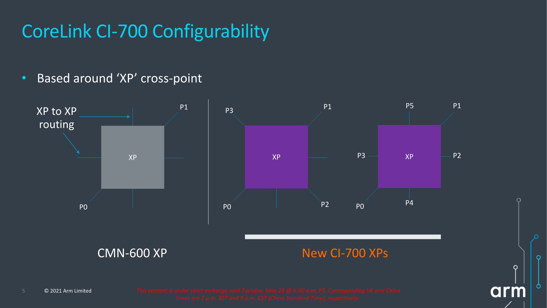
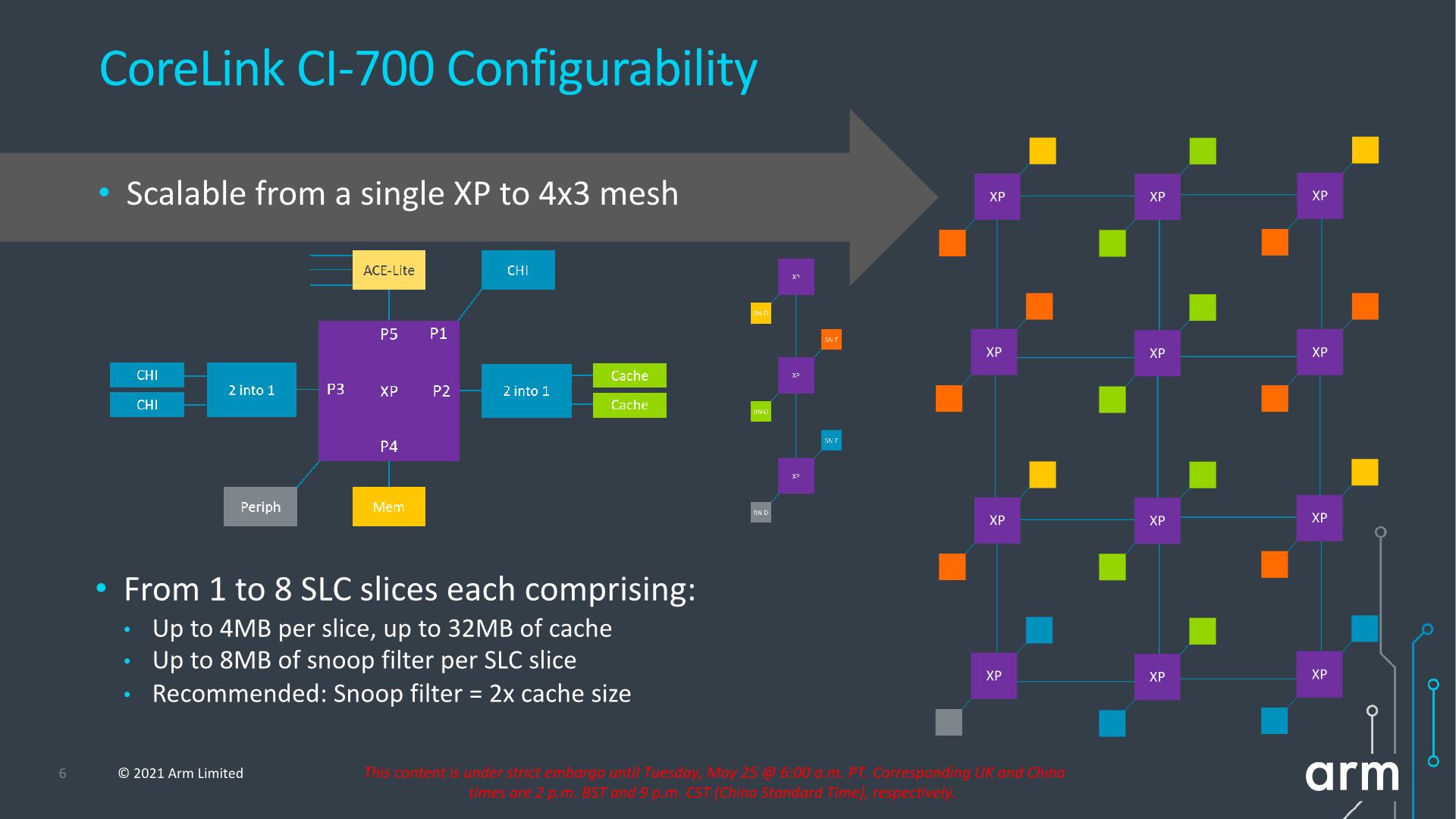
The mesh network topology and building blocks is very similar to what we’ve seen in the CMN infrastructure IP, in that “points” in the mesh are comprised of “cross-points” or “XP”. One differentiation that’s unique to the client mesh implementation is that XPs can have more attached connectivity ports, trading in routing connection paths. The new IP can also be configured as just a sole XP with no real mesh so to speak of, or essentially a 1x1 mesh configuration. This can grow up to a 4x3 mesh in the largest possible configuration.
The mesh supports from 1 to 8 SLC slices, with up to 4MB per slice for a total of 32MB, and snoop filter SRAM with coverage of up to 8MB address space per slice. It’s noted that generally Arm recommends 1.5-2x of coverage of the underlying private cache hierarchies of the mesh clients.
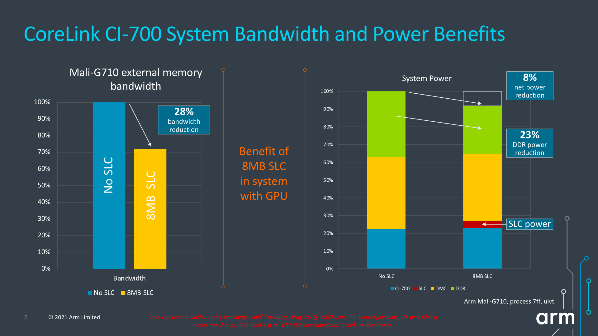
The SLC can server as both a bandwidth amplifier as well as reducing external memory/DRAM transactions, reducing system power reduction.
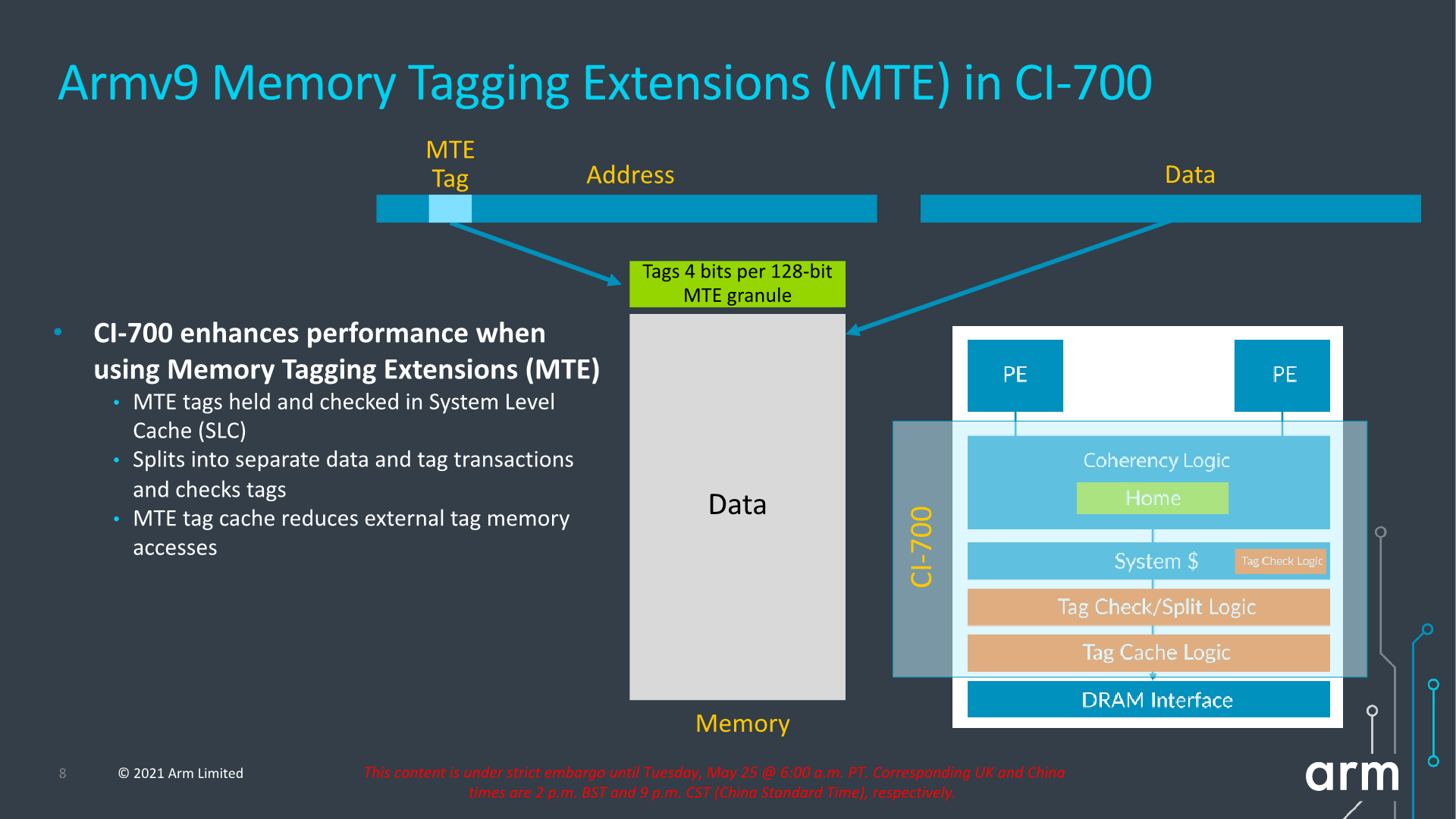
We see a reiteration of the support for MTE, allowing for this generation of IPs to support the feature across the new CPU IP, the DSU, and the new cache coherent interconnect.
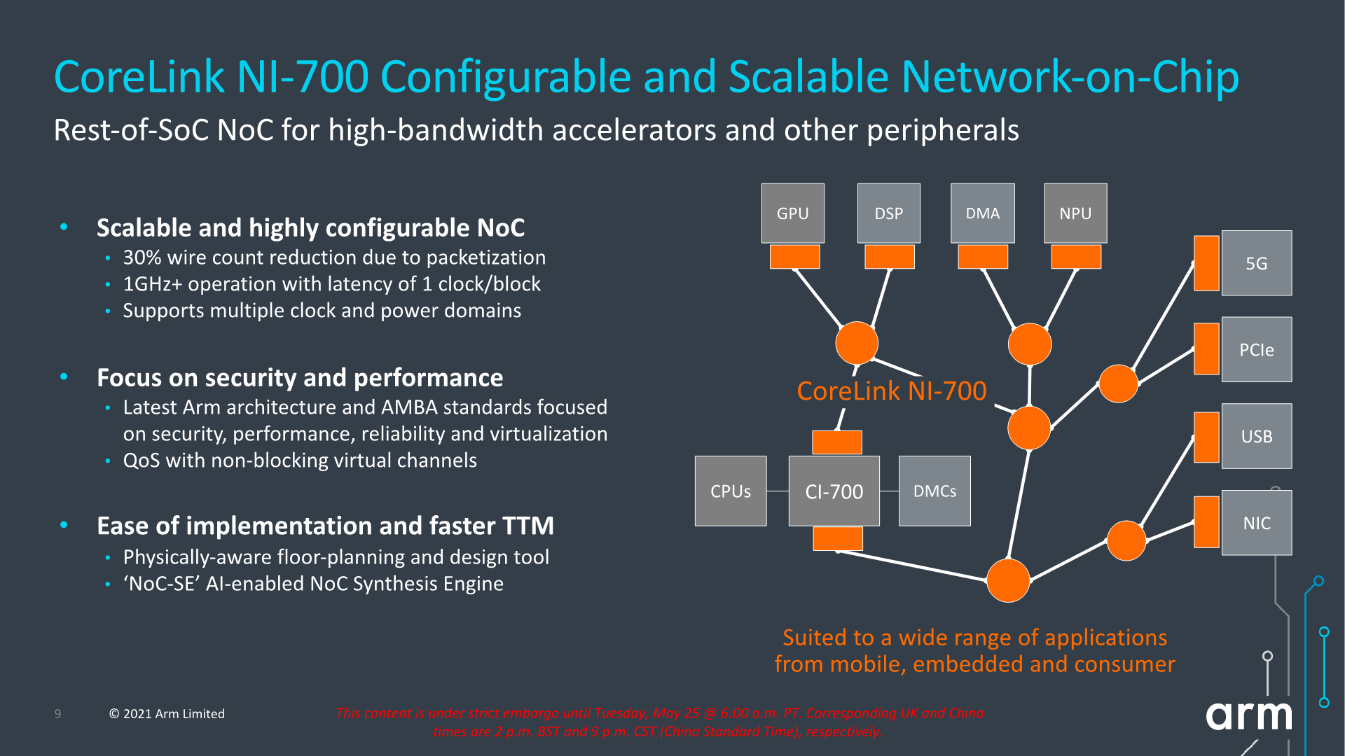
Alongside the new CI-700 coherent interconnect, we’re also seeing a new NI-700 network-on-chip for non-coherent data transfers between a SoC’s various IP blocks. The big new improvements here is the introduction of packetization for data transfers, which leads to a reduction of wires and thus improves area efficiency of the NoC on the SoC.
Overall, the new system IP announced today is very interesting, but the one question that’s one has to ask oneself is exactly who these net interconnects are meant for. Over the last few years, we’ve seen essentially every major mobile vendor roll out their own in-house cache-coherent interconnect IP, such as Samsung’s SCI or MediaTek’s MCSI, and other times we don’t see vendors talk about their in-house interconnects at all (Qualcomm). Due to almost everybody having their own IP, I’m not sure what the likelihood would be that any of the big players would jump back to Arm’s own solutions – if somebody were to adopt it, it would rather be amongst the smaller name vendors and newcomers to the market. From a business and IP portfolio perspective, the new designs make a lot of sense and allows to have the building blocks to create a mostly Arm-only SoC, which is an important item to have on the menu for Arm’s more diverse customer base.


181 Comments
View All Comments
mode_13h - Tuesday, June 1, 2021 - link
> some CPUs did mark the instruction boundaries in the cache.Not surprising, other than how far back you say it went.
mode_13h - Wednesday, May 26, 2021 - link
All good points. People who think "ISA doesn't matter" don't really understand everything an ISA encompasses.GeoffreyA - Wednesday, May 26, 2021 - link
The difference that divides them is that CISC can include a memory operation as part of an arithmetic one, whereas in RISC the two are separate (at least, in a load-store architecture).mode_13h - Wednesday, May 26, 2021 - link
> The difference that divides them is that CISC can include a memory operationI'm not an expert on the subject, but there are other elements in RISC orthodoxy, concerning things like:
* number of operands (also number of src & dst operands)
* encoding of immediates
* side-effects
I view the whole subject of CISC vs. RISC as something like MMA (Mixed Martial Arts). It turns out that there's no single best classical martial arts style. The most effective fighters use a blend of techniques adopted from various, disparate fighting styles.
GeoffreyA - Thursday, May 27, 2021 - link
"The most effective fighters use a blend of techniques"Absolutely. It's almost a universal principle that the winning design puts together the best elements from competing designs and throws away the junk.
Thala - Tuesday, May 25, 2021 - link
It does not matter that they are RISC-like inside, the issue with x86 is that they still carry the typical CISC baggage - and no internal RISC-like structure will help them here.km1810vm4 - Wednesday, May 26, 2021 - link
I would say x86 baggage. There were much nicer CISC architectures around at the time, like the Motorola 68000.TheinsanegamerN - Wednesday, May 26, 2021 - link
Intel's p5 processors implemented RISC style micro ops into their x86 decoding, that's part of why they were so dramatically faster then 486. It's not like this is hard to find out....mode_13h - Thursday, May 27, 2021 - link
> Intel's p5 processors implemented RISC style micro ops into their x86 decodingIn fact, early CPUs used a lot of microcode, and one of the ways they got faster was by replacing microcoded operations with hardwired logic. This was enabled by ever-increasing transistor budgets.
> that's part of why they were so dramatically faster then 486.
This feels like a bit of revisionist history. Here are some of the reasons why Pentium was faster than 80486:
https://en.wikipedia.org/wiki/P5_(microarchitectur...
Kamen Rider Blade - Tuesday, May 25, 2021 - link
Android needs to get their developers to stop using Java and use C/C++/Rust for their apps to eek out the max performance possible.Apple's App code base is generally C/C++, that's why they have the performance that they have.
And it's a long time nagging issue that I wish the Android community would solve.
It would give Android a HUGE performance boost to move their Apps over to C/C++/Rust.
Programming Languages have already been benchmarked against each other to see which one's faster and sorry to say it, but the C/C++/Rust family win the day in terms of Code Speed while using the same hardware platform.
https://benchmarksgame-team.pages.debian.net/bench...