Arm Announces Mobile Armv9 CPU Microarchitectures: Cortex-X2, Cortex-A710 & Cortex-A510
by Andrei Frumusanu on May 25, 2021 9:00 AM EST- Posted in
- SoCs
- CPUs
- Arm
- Smartphones
- Mobile
- Cortex
- ARMv9
- Cortex-X2
- Cortex-A710
- Cortex-A510
A new CI-700 Coherent Interconnect & NI-700 NoC For SoCs
Finally, the last new announcement of the day is a new interconnect and network-on-chip generation. The last time Arm had announced a mobile/client interconnect was back in in 2015 with the CCI-550. The reason for the large gap between IPs, in Arm’s own words, is that ever since Arm’s introduction of the DSU in its CPU complexes, there really hasn’t been any need for a cache coherent interconnect in the market. While that’s eyebrow-raising from a GPU perspective, it makes perfect sense from a CPU perspective, as coherency between CPU cores was the primary driver for such interconnects until then.
With the advent of new more complex computing platforms, such as NPUs, accelerators, and hopeful more use of GPUs in cache-coherent fashions, Arm saw a need gap in its portfolio and decided to update its client-side interconnect IP.
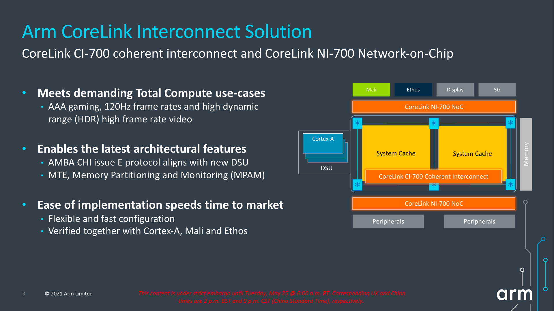
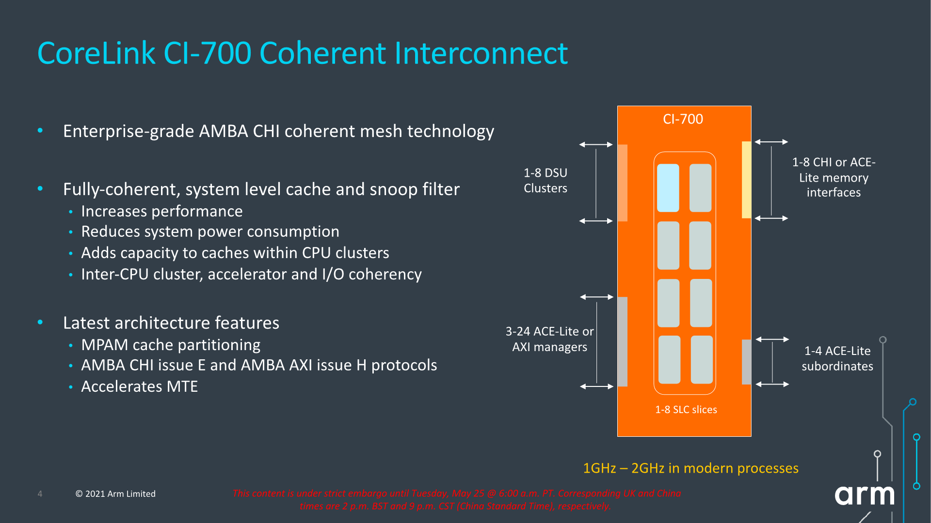
The new CI-700 is a mobile and client optimised variant of Arm’s infrastructure CMN mesh network, implementing important new interoperability with the new IP announced today, such as the new DSU or CPU cores.
The new mesh interconnect scales up from 1 to 8 DSU clusters, and supports up to 8 memory controllers, and also introduces innovations such as a system level cache.
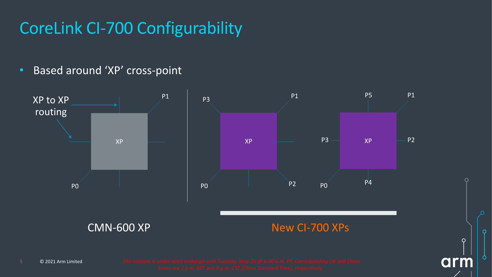
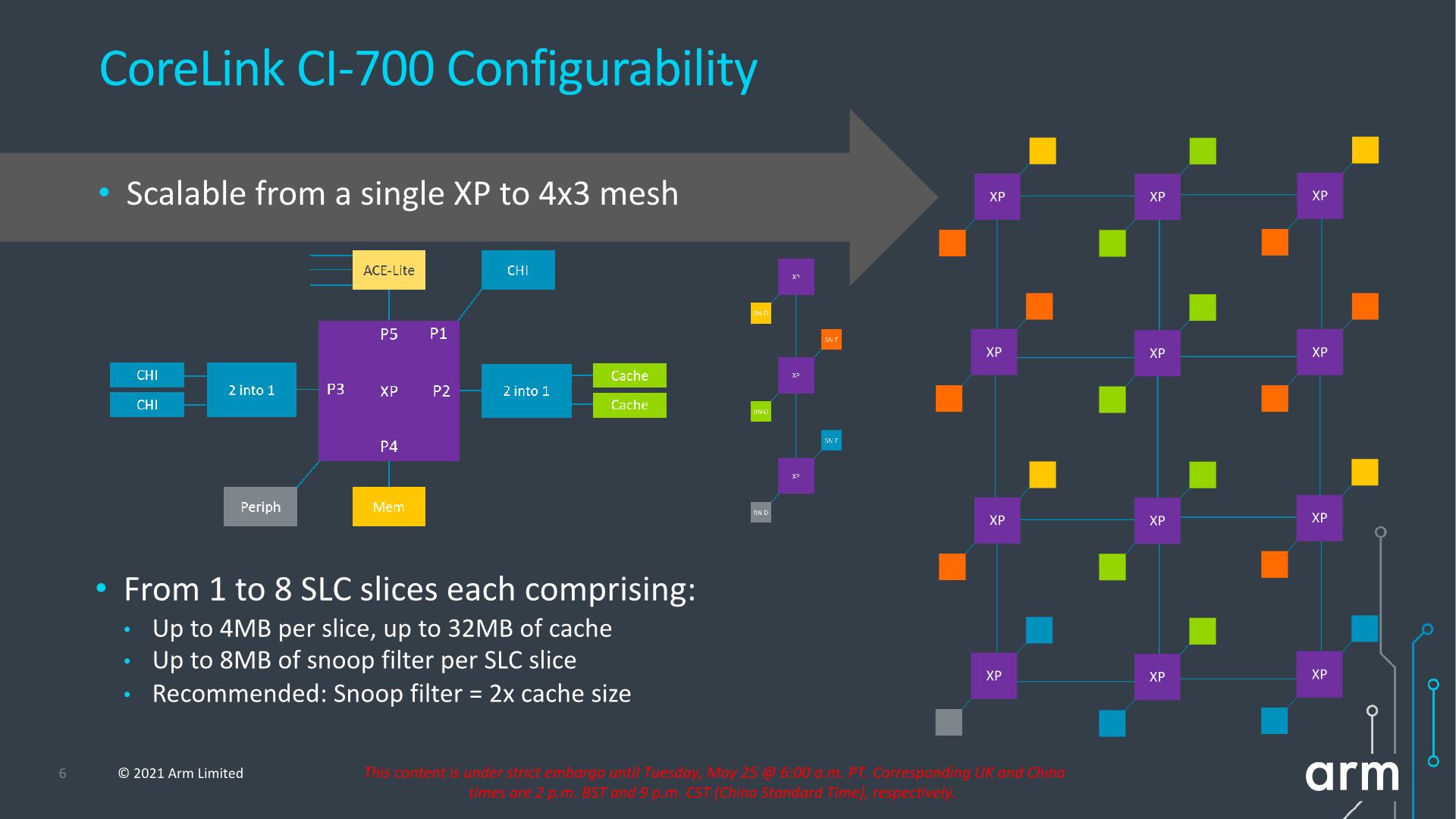
The mesh network topology and building blocks is very similar to what we’ve seen in the CMN infrastructure IP, in that “points” in the mesh are comprised of “cross-points” or “XP”. One differentiation that’s unique to the client mesh implementation is that XPs can have more attached connectivity ports, trading in routing connection paths. The new IP can also be configured as just a sole XP with no real mesh so to speak of, or essentially a 1x1 mesh configuration. This can grow up to a 4x3 mesh in the largest possible configuration.
The mesh supports from 1 to 8 SLC slices, with up to 4MB per slice for a total of 32MB, and snoop filter SRAM with coverage of up to 8MB address space per slice. It’s noted that generally Arm recommends 1.5-2x of coverage of the underlying private cache hierarchies of the mesh clients.
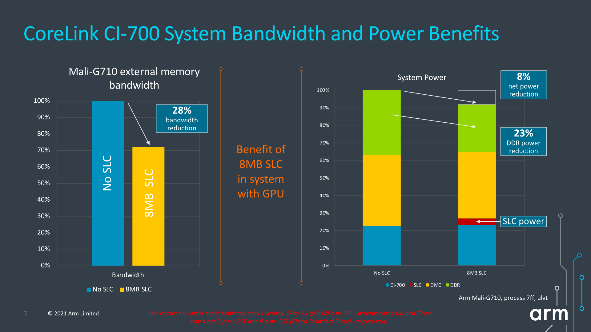
The SLC can server as both a bandwidth amplifier as well as reducing external memory/DRAM transactions, reducing system power reduction.
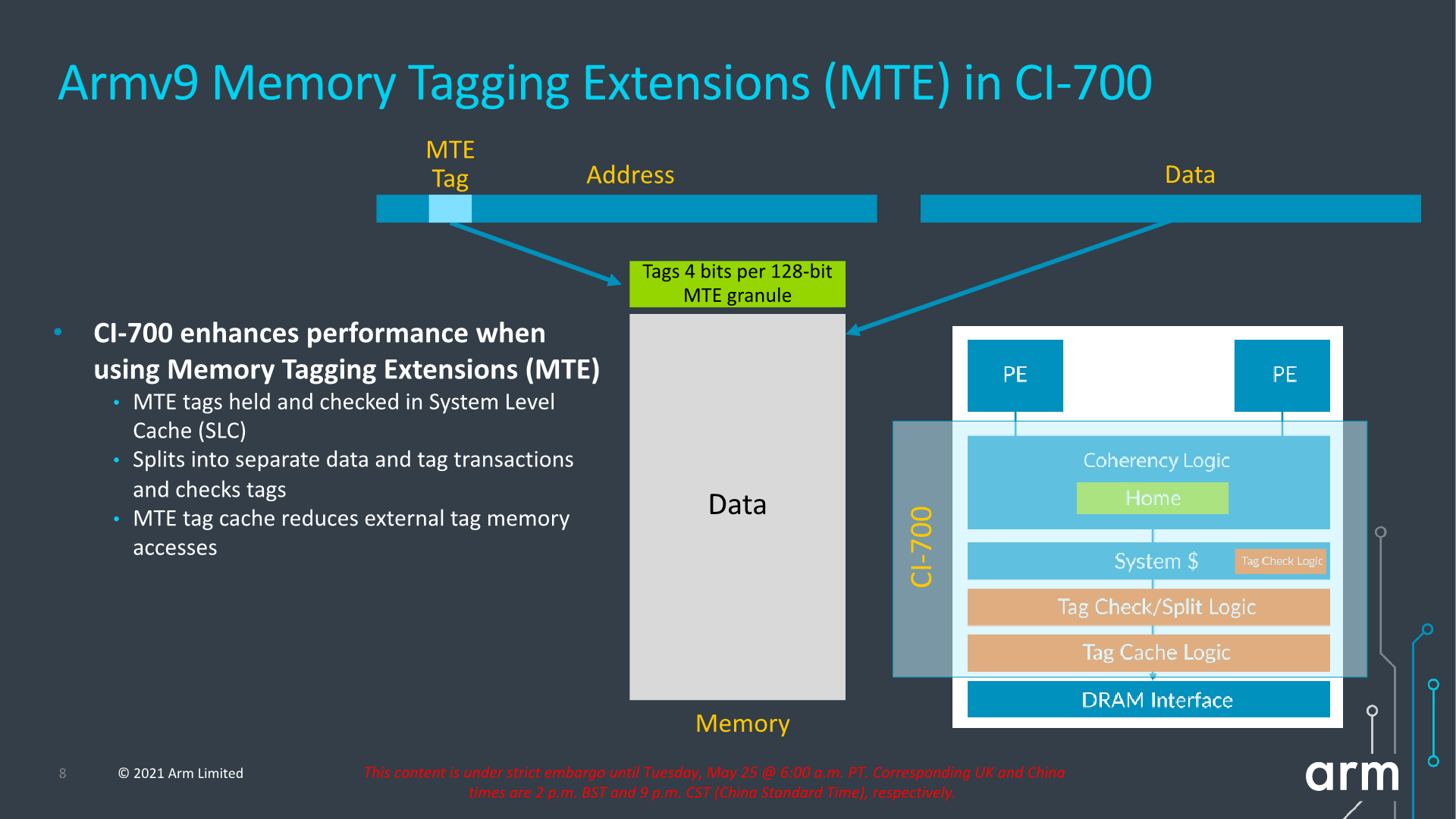
We see a reiteration of the support for MTE, allowing for this generation of IPs to support the feature across the new CPU IP, the DSU, and the new cache coherent interconnect.
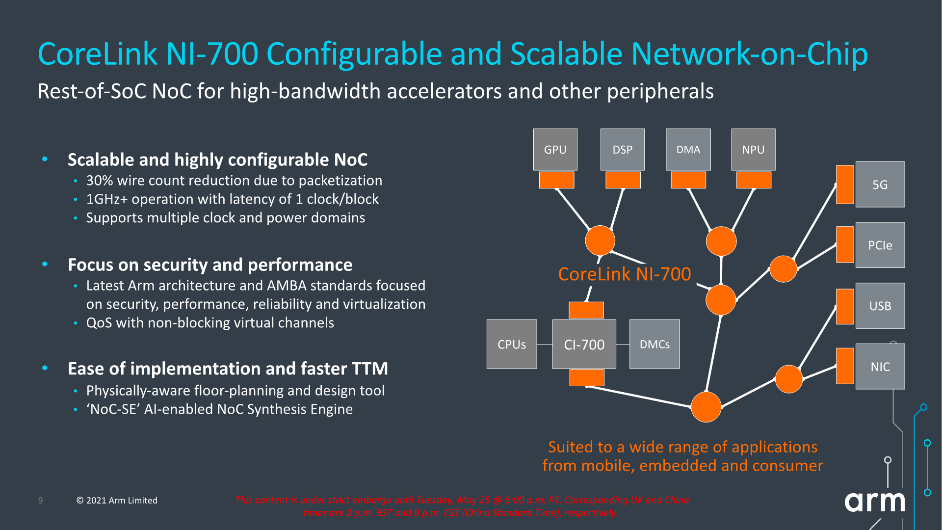
Alongside the new CI-700 coherent interconnect, we’re also seeing a new NI-700 network-on-chip for non-coherent data transfers between a SoC’s various IP blocks. The big new improvements here is the introduction of packetization for data transfers, which leads to a reduction of wires and thus improves area efficiency of the NoC on the SoC.
Overall, the new system IP announced today is very interesting, but the one question that’s one has to ask oneself is exactly who these net interconnects are meant for. Over the last few years, we’ve seen essentially every major mobile vendor roll out their own in-house cache-coherent interconnect IP, such as Samsung’s SCI or MediaTek’s MCSI, and other times we don’t see vendors talk about their in-house interconnects at all (Qualcomm). Due to almost everybody having their own IP, I’m not sure what the likelihood would be that any of the big players would jump back to Arm’s own solutions – if somebody were to adopt it, it would rather be amongst the smaller name vendors and newcomers to the market. From a business and IP portfolio perspective, the new designs make a lot of sense and allows to have the building blocks to create a mostly Arm-only SoC, which is an important item to have on the menu for Arm’s more diverse customer base.


181 Comments
View All Comments
jeremyshaw - Tuesday, May 25, 2021 - link
Something I'm not quite catching with the DSU, does it allow for different configurations that we've already seen? Something like the 8xA78C we saw announced a while back?jeremyshaw - Tuesday, May 25, 2021 - link
*than, sorrySarahKerrigan - Tuesday, May 25, 2021 - link
They show 8x X2 configs, so I'd be shocked if 8xA710 was not also on the menu.igor velky - Tuesday, May 25, 2021 - link
first two slides on page 5 will give you answer,both slides show cpu cores inside one cpu cluster
first slide shows different cores,
second shows only one type of core in cpu cluster
on page 6 because of bad formatting there are two slides looking like one picture
so second slide, bottom half of first picture
shows you that you can put max 8 cpu clusters to one chip.
so you can have
max 8 cpu cores per cpu cluster
times
8 cpu clusters per one chip.
you choose cores, you choose how many cores, you choose which type of cores, you choose how many memory channels, you choose how many and what type of additional accelerators you put inside chip...
because youre apple, samsung, qualcomm...
and you choose this things and let someone to "etch it" into silicon.
and you then sell it.
melgross - Tuesday, May 25, 2021 - link
Well, Apple doesn’t “choose” cores, they design them from scratch.Linustechtips12#6900xt - Wednesday, May 26, 2021 - link
ehhh, they get the IP for cores like the x1 or a76 then they tweak them either a lot or a little and create their current "firestorm/Icestorm" coresmichael2k - Wednesday, May 26, 2021 - link
Sure, they tweak them a lot, just like I tweaked your post a lot to make my own. The A13 released in 2019 was an 8 wide CPU; in comparison the state of the art A76 at the time was only a 4 wide CPU. That’s a pretty big deal.The X1 has an 8 wide dispatch, meaning it can issue 8 Mops per cycle but only decode 5 instructions per cycle. This is 2 years after Apple released the A13 which was 8 wide dispatch and decode. If you look at Anandtech’s A14 article you see that Apple has made the Icestorm cores roughly equivalent to an A76 since it is a 3 wide out of order design.
You can read more here:
https://www.anandtech.com/show/16226/apple-silicon...
mattbe - Wednesday, May 26, 2021 - link
This is complete BS. They license the ISA from ARM. They DO NOT USE OR TWEAK cores like the X1 and A76 to create their firestorm/ice storm cores. These are information that can easily be verified so it's pretty ignorant for you to make those claims.FunBunny2 - Wednesday, May 26, 2021 - link
" They DO NOT USE OR TWEAK cores"near as I can tell, most 'innovation' in cpu design/engineering has been, for years, throwing ever expanding transistor budgets (can we expect that to continue?) at register width, path width, buffer/cache width and number, pulling off-chip function on-chip. and the like. if Apple should ever publish the full spec of one of these chips, will we see that they've done anything more 'innovative' than Bigger, Wider, More?
all of the 'innovation' cited by michael2k fits that bill.
mode_13h - Thursday, May 27, 2021 - link
> if Apple should ever publish the full spec of one of these chips,> will we see that they've done anything more 'innovative' than Bigger, Wider, More?
You don't get perf/W numbers like Apple's by simply doing "bigger, wider, more".
There's information out there about some of their tricks, if you're willing to look for it. But I understand that it takes work and why do that, when you're perfectly content in your belief that there's nothing new under the sun?