Intel 3rd Gen Xeon Scalable (Ice Lake SP) Review: Generationally Big, Competitively Small
by Andrei Frumusanu on April 6, 2021 11:00 AM EST- Posted in
- Servers
- CPUs
- Intel
- Xeon
- Enterprise
- Xeon Scalable
- Ice Lake-SP
Topology, Memory Subsystem & Latency
The topologies of the new Ice Lake-SP parts are quite straightforward when it comes to their generational evolution from Cascade Lake-SP. The most important thing of note here is that this generation’s HCC (high core count) die employed by Intel is of the same core count as last generation’s XCC die – 28 cores. The new ICX XCC die is now at 40 cores, with the Xeon 8380 we’re testing today being of this flavour.
Unfortunately, Intel didn’t specify which SKUs use XCC dies and which use HCC, only disclosing that XCC goes up to 40 cores, and HCC goes up to 26 cores. We also have a Xeon 6330 available for testing at 28 cores, meaning that also would be of the XCC design.
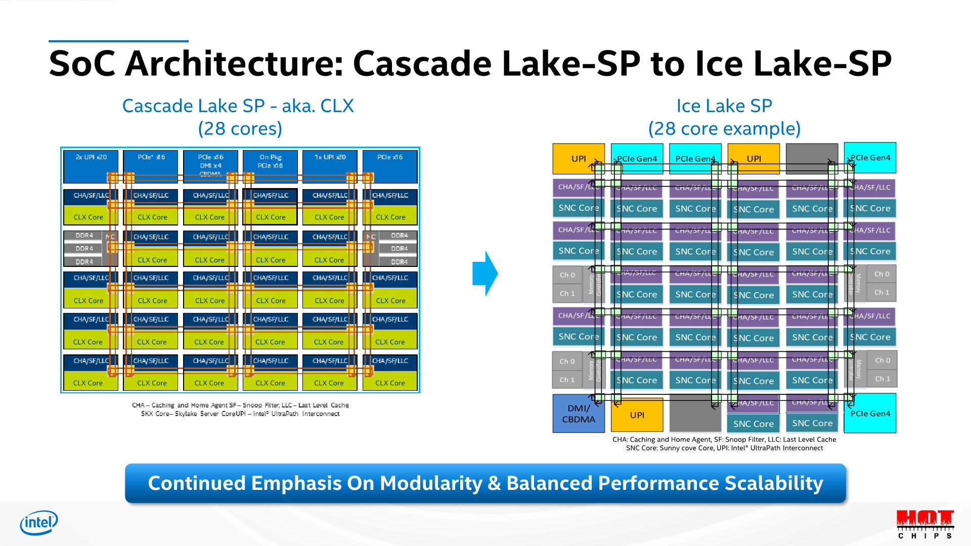
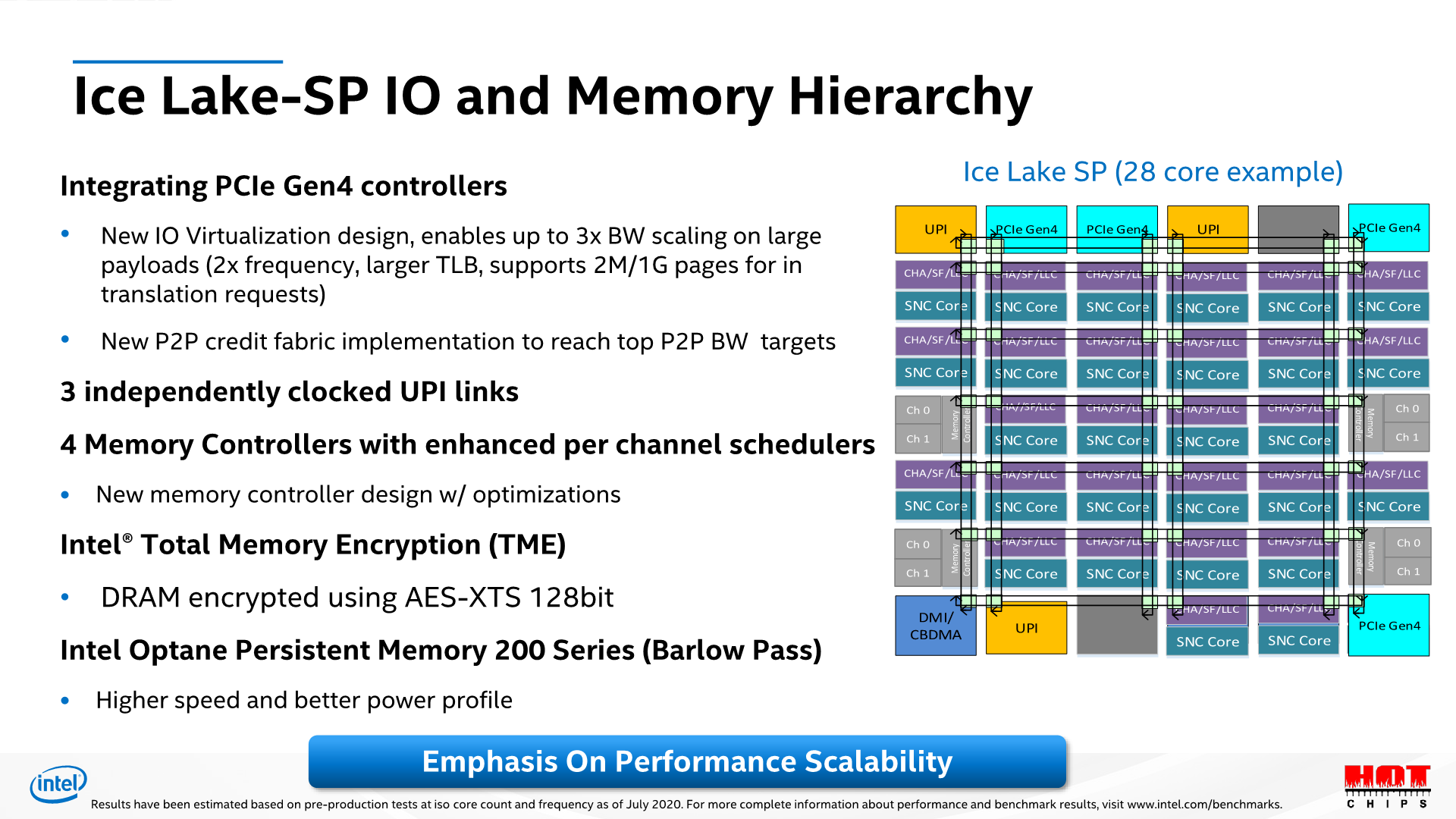
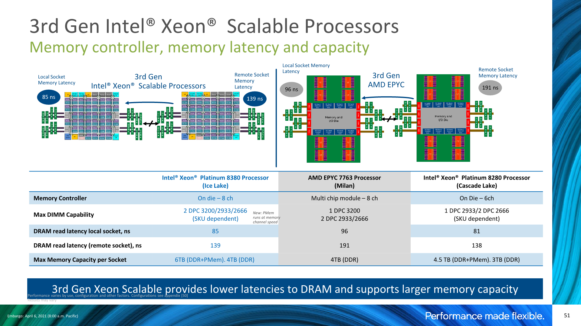
At the heart, Ice Lake SP is still a monolithic mesh design, with a few differences in the composition of the blocks, such as rearranged UPI positioning, extra 16 PCIe lanes which have been upgraded to 4.0 capability, as well as most importantly the move from a 2-memory controller design with 3-channel granularity, to a 4-controller design with 2-channel granularity, which makes for an important distinction later on in the memory performance of the system.
Starting off with our core-to-core test, the test consists of two threads atomically altering a value on a shared cache line before the threads are spawned from a main housekeeping thread. In essence we’re measuring hardware core-to-cacheline-to-core as well as the hardware coherency round-trip time for the data to be visible from one core to another. Such core-to-core latencies are important in multi-threaded workloads which have lots of shared data operations, such as databases.

At first glance, we’re not seeing all that much different latencies within a socket, however we have to remind ourselves that we’re comparing boost clocks of up to 4GHz on the Cascade Lake SP based Xeon 8280, while our Ice Lake SP Xeon 8380 only boosts up to 3.4GHz. In that regard, maintaining similar core-to-core latencies all whilst increasing the mesh size from 28 cores to 40 cores is actually quite impressive – there is a slight degradation of a few nanoseconds but generally it’s not something overly significant.
What’s a bit odd is the larger latencies between core N to core N+1 at +60ns. What’s even more odd, is that this only ever happens when we measure from physical core N to physical core N+1 on the same enumerated logical CPU, if we actually measure from physical core N to the other logical CPU of physical N+1 then we’re getting normal access latencies as any other combination of physical and logical cores. I’ve got no idea what’s happening here but the measurements seem to be consistent in their behaviour.
The major improvement on Ice Lake seems to be socket-to-socket latencies, which in our measurements have gone down from ~135ns to ~108ns on these particular SKUs at these particular frequencies. That’s a major generational improvement, and further advances Intel’s leadership position in this metric. In fact, the new Xeon 8380’s socket-to-socket latencies are now essentially the same as what AMD has to incur within a single socket between cores in different IOD quadrants, with cores within a quadrant only being slightly faster. AMD’s socket-to-socket latencies naturally fall far behind at around ~190ns, even with the newer Milan based designs which had notably improved upon this metric compared to Rome.
Memory Latency
As noted, the one big change this generation is that the CPU moves from a dual 3-channel memory controller to a quad 2-channel memory controller setup, increasing total available theoretical peak memory bandwidth by 45% through the 33% increase in memory channels, as well as the DRAM frequency increase from DDR4-2933 to DDR-3200.
Counteracting the new controller redesign is however the fact that this is simply a bigger chip, so data has to go through more mesh nodes to reach their destination as well as memory controllers.
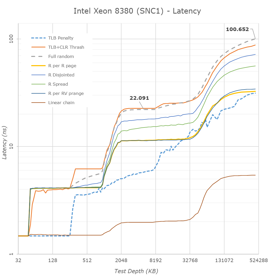
Looking at the test results with the chip in a monolithic NUMA configuration, we’re seeing the new chip slightly regress in its latencies, which actually was to be expected given the clock frequency differences between the generation SKUs. It’s not a major disadvantage, however something to keep in mind for later tests. With Intel slightly regressing, and AMD having greatly improved memory latencies in Milan, the gap between the two competitors is smaller than in previous generations where Intel had a more formidable lead.
Intel’s presentations disclosed similar figures, although they’re using a different measuring methodology with MLC and simple patterns with prefetchers disabled, whereas we simply measure full random latency including TLB misses.
We weren’t able to verify the claim, but Intel also advertises advantages in remote socket DRAM latencies. The difference here matches what we’re seeing with the core-to-core latency tests, but it’s a bit of an oddball metric as I have trouble thinking of workloads where this would matter much, unless you’re running a single NUMA node across two sockets, which should be rare.
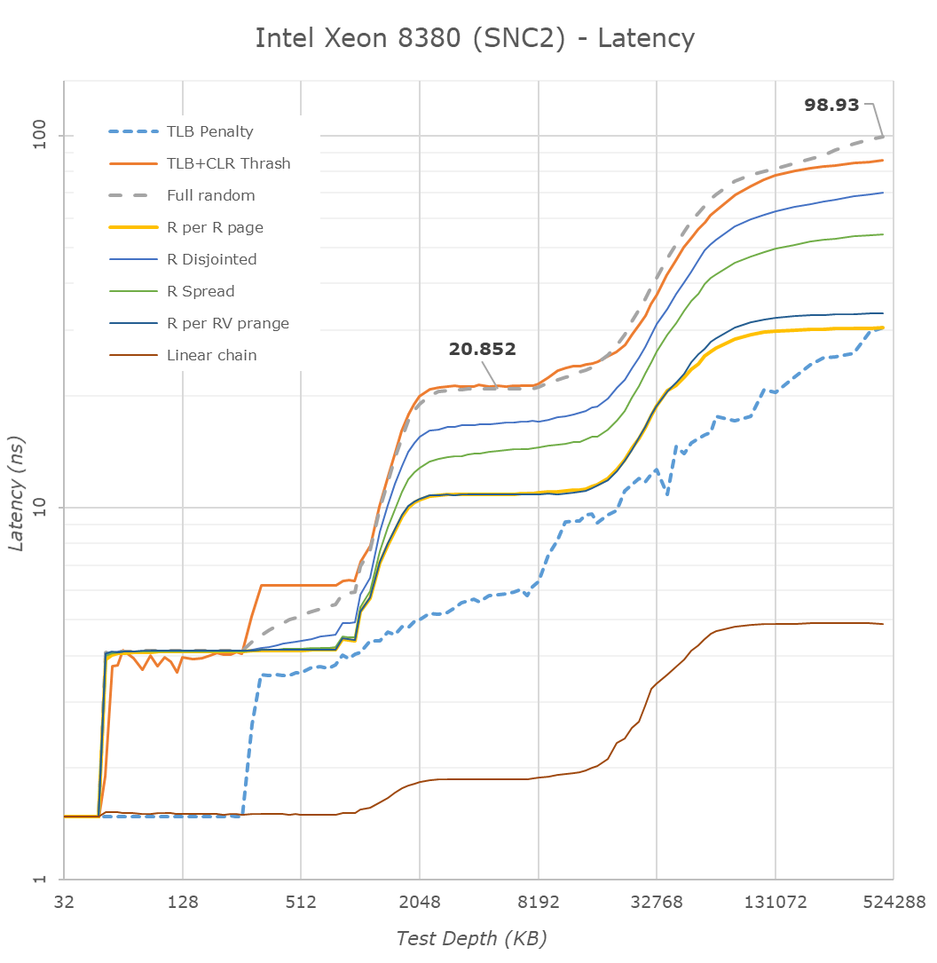
Intel had sub-NUMA clustering in prior generations, however the bigger a chip is and the larger the core count, the more these setup configurations are expected to have a difference in performance and latencies. Running the chip in SNC2 mode, meaning splitting the chip into two NUMA domains, splits the mesh into two logical parts, halving the L3 accessible to a single core, and each half only having access to their local memory controllers.
DRAM latencies here are reduced by 1.7ns, which isn’t very much a significant difference, and the L3 latencies go down by 1.2ns which is around a 5.9% reduction.
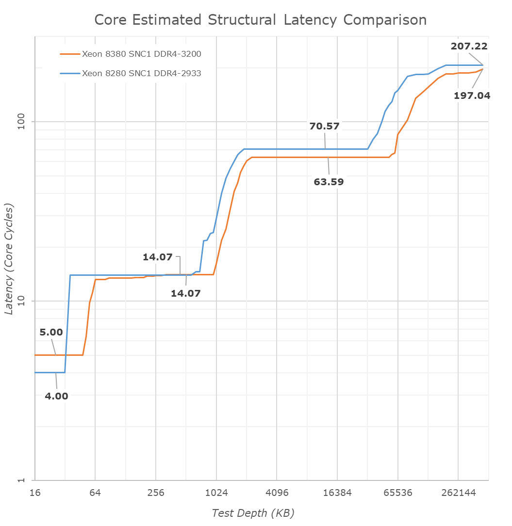
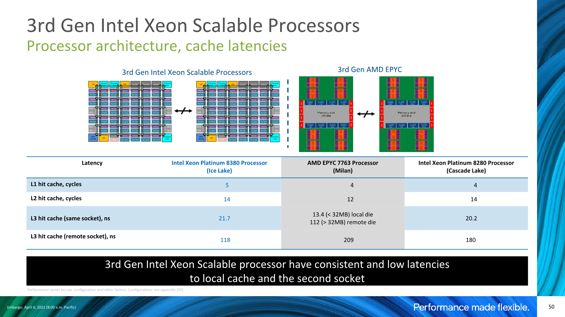
Looking at access latencies from a core cycle view, the new Ice Lake SP system is actually quite impressive. The L1 does regress from 4 to 5 cycles with the increase from 32KB to 48KB, however the L2 remains at the same 14 cycles even though it has grown from 1MB to 1.25MB.
What Intel didn’t mention in their presentation as much is that although the absolute latencies in the L3 mesh has slightly regressed from the 8280 to the new 8380, on a core clock cycle basis, it’s actually faster as we’re measuring a reduction from an average 70.5 cycles down to 63.5 cycles, which is a very impressive feat given that the mesh now contains 42% more cores, and increases its size from 38.5MB at 1.375MB/slice to 60MB at 1.5MB/slice.
Memory Bandwidth
In terms of memory bandwidth, we’re falling back to the standard STREAM benchmark, in particular the Triad test which is a simple streaming memory compute test. As I had talked about more extensively in our Ampere Altra review, I find it much more interesting to test the scaling bandwidth with increasing thread count in a system as it can reveal much more nuances of system behaviour than just a simple single figure at the arbitrary maximum thread count.
We’re also using a vanilla compilation of STREAM with GCC without any explicit optimisations that alter memory operations types, as this way it’s a more realistic representation of how most generic workloads will behave on a system.
STREAM Triad is a simple test consisting of a a[j] = b[j]+scalar*c[j]; compute kernel iterating over three memory arrays. The test assumes 3 memory operations: two memory reads and one memory write. From a hardware perspective, this can actually be 4 memory operations as many cores have to first read out a content of a target cache-line before writing to it.
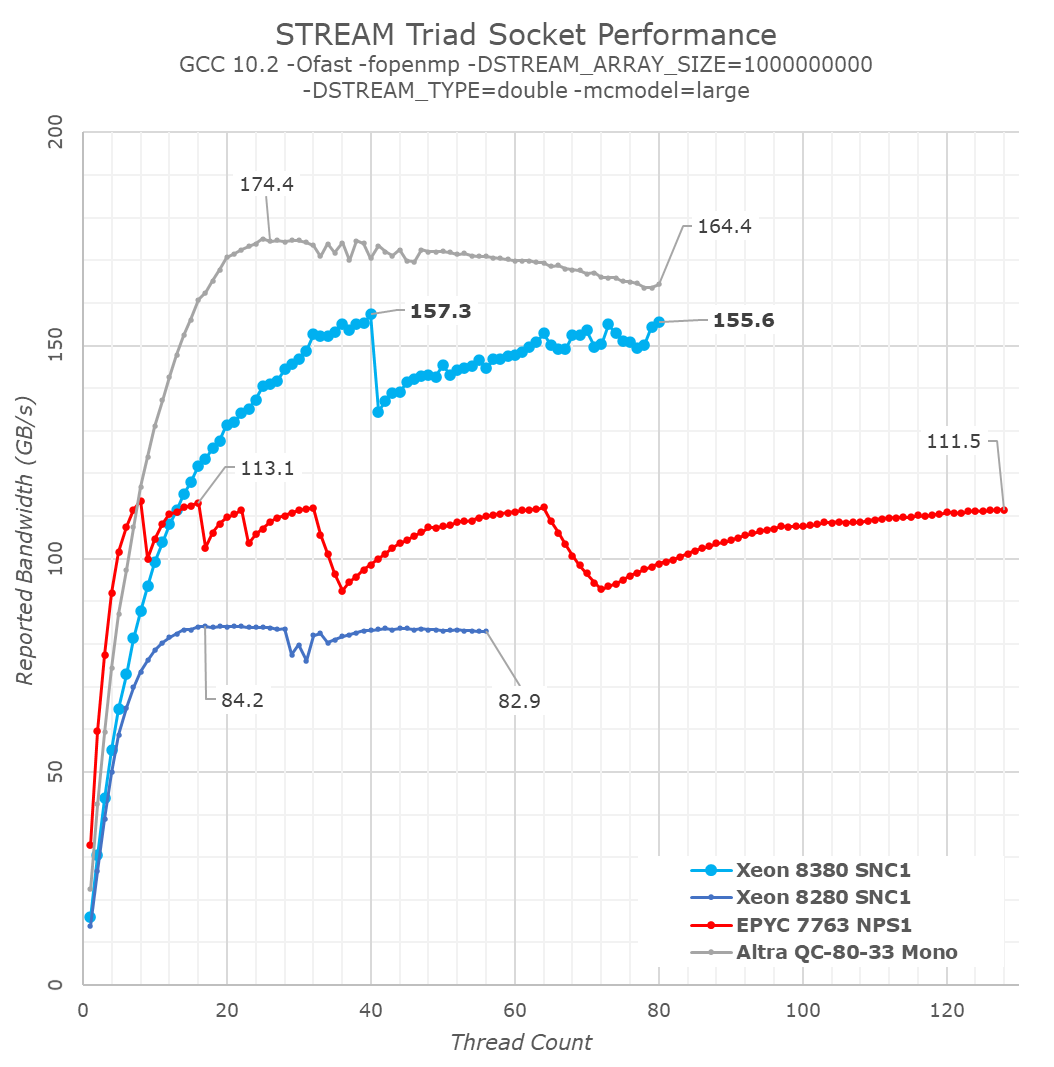
Generally, what we were expecting with Ice Lake SP were figures that were +45% ahead of Cascade Lake SP, thanks to the improved memory controllers and more memory channels. Instead, what we’re seeing here are improvements reaching up to +86%, well beyond the figures we were expecting.
As per the data, the new ICX design appears to be vastly outperforming its predecessor, and also essentially leaving AMD trailing far behind in terms of raw memory performance, only falling behind Ampere’s Altra which is able to dynamically detect streaming memory workloads and transform memory operations into non-temporal ones.
What’s also to be noted is that the per-core bandwidth this generation doesn’t seem to have improved very much from Cascade Lake SP, with AMD’s newest Milan still vastly outperforming Ice Lake SP at lower thread counts, and single-core bandwidth being much higher on the competitor systems.
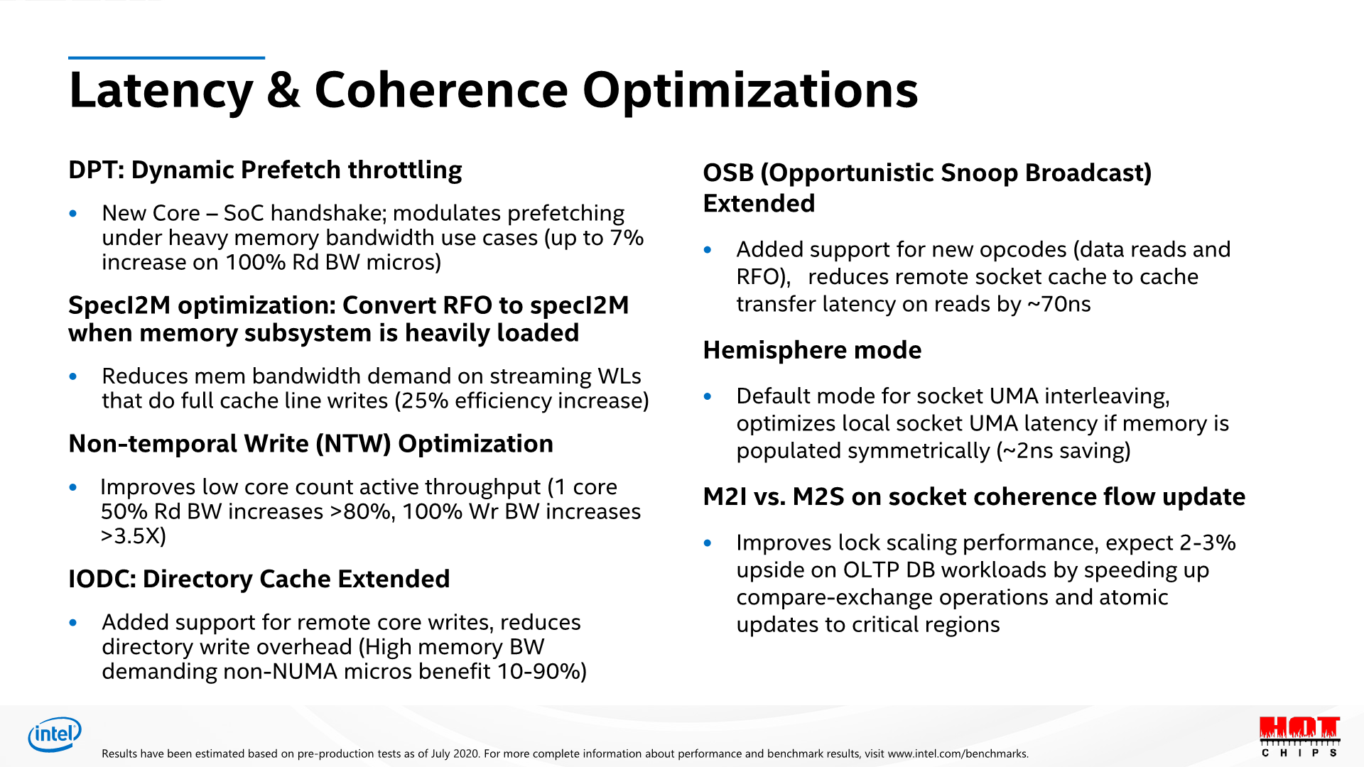
Inspecting Intel’s prior disclosures about Ice Lake SP in last year’s HotChips presentations, one point sticks out, and that is the “SpecI2M optimisation”, where the system is able to convert traditional RFO (Read for ownership) memory operations into another mechanism. We don’t know exactly what SpecI2M does, but Intel does disclose that it’s meant to optimise bandwidth and data traffic under streaming workloads. It doesn’t seem that this is a full kind of memory operation transformation into non-temporal writes as on the Arm systems we’ve seen lately, but it does significantly boost the bandwidth well beyond what we’ve seen of other x86 systems.
It’s a bit unfortunate that system vendors have ended up publishing STREAM results with hyper optimised binaries that are compiled with non-temporal instructions from the get-go, as for example we would not have seen this new mechanism on Ice Lake SP with those kind of binaries. Intel themselves are only disclosing a +47% increase in STREAM Triad performance – I consider the real-world improvement to be significantly higher than that figure, as this new dynamic mechanism doesn’t depend on specifically tuned software.
Overall, Intel’s overall larger mesh, new memory controllers, and architectural improvements in regards to memory bandwidth are absolutely impressive, and well beyond what I had expected of this generation. The latter STREAM results were really great to see as I view it as a true design innovation that will benefit a lot of workloads.


169 Comments
View All Comments
TomWomack - Wednesday, April 7, 2021 - link
Is it known whether there will be an IceLake-X this time round? The list of single-Xeon motherboard launches suggests possibly not; it would obviously be appealing to have a 24-core HEDT without paying the Xeon premium.EthiaW - Wednesday, April 7, 2021 - link
Boeings and Airbuses are never actually sold at their nominal prices, they cost far less, a non-disclosed number, for big buyers after gruesome haggling, sometimes less than half the “catalogue” price.I think this is exactly what's intel doing now: set the catalogue price high to avoid losing face, and give huge discount to avoid losing market share.
duploxxx - Wednesday, April 7, 2021 - link
well easy conclusion.EPYC 75F3 is the clear winner SKU and the must have for most of the workloads.
This is based on price - performance - cores and its related 3rd party sw licensing...
I wonder when Intel will be able to convince VMware to move from a 32core licensing schema to a 40core :)
They used to get all the dev favor when PAT was still in the house, I had several senior engineers in escalation calls stating that the hypervisor was optimised for Intel ...guess what even under optimised looking for a VM farm in 2020-2021-....you are way better off with an AMD build.
WaltC - Wednesday, April 7, 2021 - link
If you can't beat the competition, then what? Ian seems to be impressed that Intel was finally able to launch a Xeon that's a little faster than its previous Xeon, but not fast enough to justify the price tag in relation to what AMD has been offering for a while. So here we are congratulating Intel on burning through wads more cash to produce yet-another-non-competitive result. It really seems as if Intel *requires* AMD to set its goals and to tell it where it needs to go--and that is sad. It all began with x86-64 and SDRAM from AMD beating out Itanium and RDRAM years ago. And when you look at what Intel has done since it's just not all that impressive. Well, at least we can dispense with the notion that "Intel's 10nm is TSMC's 7nm" as that clearly is not the case.JayNor - Wednesday, April 7, 2021 - link
What about the networking applications of this new chip? Dan Rodriguez's presentation showed gains of 1.4x to 1.8x for various networking benchmarks. Intel's entry into 5G infrastructure, NFV, vRAN, ORAN, hybrid cloud is growing faster than they originally predicted. They are able to bundle Optane, SmartNICs, FPGAs, eASIC chips, XeonD, P5900 family Atom chips... I don't believe they have a competitor that can provide that level of solution.Bagheera - Thursday, April 8, 2021 - link
Patr!ck Patr!ck Partr!ck?evilpaul666 - Saturday, April 10, 2021 - link
It only works in front of a mirror. Donning a hoodie helps, too.Oxford Guy - Wednesday, April 7, 2021 - link
There is some faulty logic at work in many of the comments, with claims like it's cheating to use a more optimized compiler.It's not cheating unless:
• the compiler produces code that's so much more unstable/buggy that it's quite a bit more untrustworthy than the less-optimized compiler
• you don't make it clear to readers that the compiler may make the architecture look more performant simply because the other architectures may not have had compiler optimizations on the same level
• you use the same compiler for different architectures when using a different compiler for one or more other architectures will produce more optimized code for those architectures as well
• the compiler sabotages the competition, via things like 'genuine Intel'
Fact is that if a CPU can accomplish a certain amount of work in a certain amount of time, using a certain amount of watts under a certain level of cooling — that is the part's actual performance capability.
If that means writing machine code directly (not even assembly) to get to that performance level, so what? That's an entirely different matter, which is how practical/economical/profitable/effortful it is to get enough code to measure all of the different aspects of the part's maximum performance capability. The only time one can really cite that as a deal-breaker is if one has hard data to demonstrate that by the time the hand-tuned/optimized code is written changes to the architecture (and/or support chips/hardware) will obsolete the advantage — making the effort utterly fruitless, beyond intellectual curiosity concerning the part's ability. For instance, if one knows that Intel, for instance, is going to integrate new instructions (very soon) that will make various types of hand-tuned assembly obsolete in short order, it can be argued that it's not worth the effort to write the code. People made this argument with some of AMD's Bulldozer/Piledriver instructions, on the basis that enough industry adoption wasn't going to happen. But, frankly... if you're going to make claims about the part's performance, you really should do what you can to find out what it is.
Oxford Guy - Wednesday, April 7, 2021 - link
One can, though, of course... include a disclaimer that 'it seems clear enough that, regardless of how much hand-tuned code is done, the CPU isn't going to deliver enough to beat the competition, if the competition's code is similarly hand-tuned' — if that's the case. Even if a certain task is tuned to run twice as fast, is it going to be twice as fast as tuned code for the competition's stuff? Is its performance per watt deficit going to be erased? Will its pricing no longer be a drag on its perceived competitiveness?For example, one could have wrung every last drop of performance out of Bulldozer but it wasn't going to beat Sandy Bridge E — a chip with the same number of transistors. Piledriver could beat at least the desktop version of Sandy in certain workloads when clocked well outside of the optimal (for the node's performance per watt) range but that's where it's very helpful to have tests at the same clock. It was discovered, for instance, that the Fury X and Vega had basically identical performance at the same clock. Since desktop Sandy could easily clock at the same 4.0 GHz Piledriver initially shipped with it could be tested at that rate, too.
Ideally, CPU makers would release benchmarks that demonstrate every facet of their chip's maximum performance. The concern about those being best-case and synthetic is less of a problem in that scenario because all aspects of the chip's performance would be tested and published. That makes cherry-picking impossible.
mode_13h - Thursday, April 8, 2021 - link
The faulty logic I see is that you seem to believe it's the review's job to showcase the product in the best possible light. No, that's Intel's job, and you can find plenty of that material at intel.com, if that's what you want.Articles like this should focus on representing the performance of the CPUs as the bulk of readers are likely to experience it. So, even if using some vendor-supplied compiler with trick settings might not fit your definition of "cheating", that doesn't mean it's a service to the readers.
I think it could be appropriate to do that sort of thing, in articles that specifically analyze some narrow aspect of a CPU, for instance to determine the hardware's true capabilities or if it was just over-hyped. But, not in these sort of overall reviews.