Intel 3rd Gen Xeon Scalable (Ice Lake SP) Review: Generationally Big, Competitively Small
by Andrei Frumusanu on April 6, 2021 11:00 AM EST- Posted in
- Servers
- CPUs
- Intel
- Xeon
- Enterprise
- Xeon Scalable
- Ice Lake-SP
Topology, Memory Subsystem & Latency
The topologies of the new Ice Lake-SP parts are quite straightforward when it comes to their generational evolution from Cascade Lake-SP. The most important thing of note here is that this generation’s HCC (high core count) die employed by Intel is of the same core count as last generation’s XCC die – 28 cores. The new ICX XCC die is now at 40 cores, with the Xeon 8380 we’re testing today being of this flavour.
Unfortunately, Intel didn’t specify which SKUs use XCC dies and which use HCC, only disclosing that XCC goes up to 40 cores, and HCC goes up to 26 cores. We also have a Xeon 6330 available for testing at 28 cores, meaning that also would be of the XCC design.
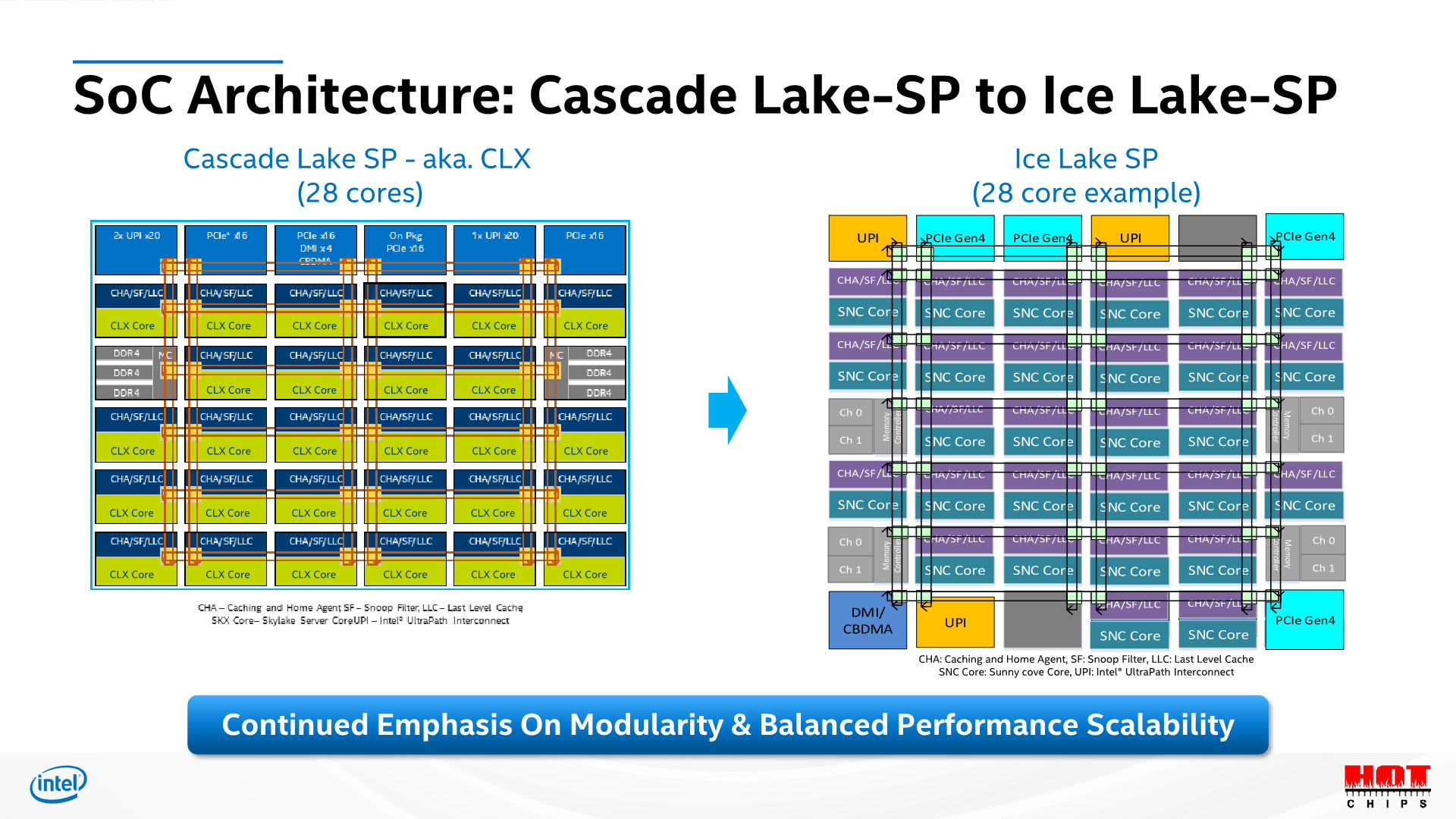
At the heart, Ice Lake SP is still a monolithic mesh design, with a few differences in the composition of the blocks, such as rearranged UPI positioning, extra 16 PCIe lanes which have been upgraded to 4.0 capability, as well as most importantly the move from a 2-memory controller design with 3-channel granularity, to a 4-controller design with 2-channel granularity, which makes for an important distinction later on in the memory performance of the system.
Starting off with our core-to-core test, the test consists of two threads atomically altering a value on a shared cache line before the threads are spawned from a main housekeeping thread. In essence we’re measuring hardware core-to-cacheline-to-core as well as the hardware coherency round-trip time for the data to be visible from one core to another. Such core-to-core latencies are important in multi-threaded workloads which have lots of shared data operations, such as databases.

At first glance, we’re not seeing all that much different latencies within a socket, however we have to remind ourselves that we’re comparing boost clocks of up to 4GHz on the Cascade Lake SP based Xeon 8280, while our Ice Lake SP Xeon 8380 only boosts up to 3.4GHz. In that regard, maintaining similar core-to-core latencies all whilst increasing the mesh size from 28 cores to 40 cores is actually quite impressive – there is a slight degradation of a few nanoseconds but generally it’s not something overly significant.
What’s a bit odd is the larger latencies between core N to core N+1 at +60ns. What’s even more odd, is that this only ever happens when we measure from physical core N to physical core N+1 on the same enumerated logical CPU, if we actually measure from physical core N to the other logical CPU of physical N+1 then we’re getting normal access latencies as any other combination of physical and logical cores. I’ve got no idea what’s happening here but the measurements seem to be consistent in their behaviour.
The major improvement on Ice Lake seems to be socket-to-socket latencies, which in our measurements have gone down from ~135ns to ~108ns on these particular SKUs at these particular frequencies. That’s a major generational improvement, and further advances Intel’s leadership position in this metric. In fact, the new Xeon 8380’s socket-to-socket latencies are now essentially the same as what AMD has to incur within a single socket between cores in different IOD quadrants, with cores within a quadrant only being slightly faster. AMD’s socket-to-socket latencies naturally fall far behind at around ~190ns, even with the newer Milan based designs which had notably improved upon this metric compared to Rome.
Memory Latency
As noted, the one big change this generation is that the CPU moves from a dual 3-channel memory controller to a quad 2-channel memory controller setup, increasing total available theoretical peak memory bandwidth by 45% through the 33% increase in memory channels, as well as the DRAM frequency increase from DDR4-2933 to DDR-3200.
Counteracting the new controller redesign is however the fact that this is simply a bigger chip, so data has to go through more mesh nodes to reach their destination as well as memory controllers.
Looking at the test results with the chip in a monolithic NUMA configuration, we’re seeing the new chip slightly regress in its latencies, which actually was to be expected given the clock frequency differences between the generation SKUs. It’s not a major disadvantage, however something to keep in mind for later tests. With Intel slightly regressing, and AMD having greatly improved memory latencies in Milan, the gap between the two competitors is smaller than in previous generations where Intel had a more formidable lead.
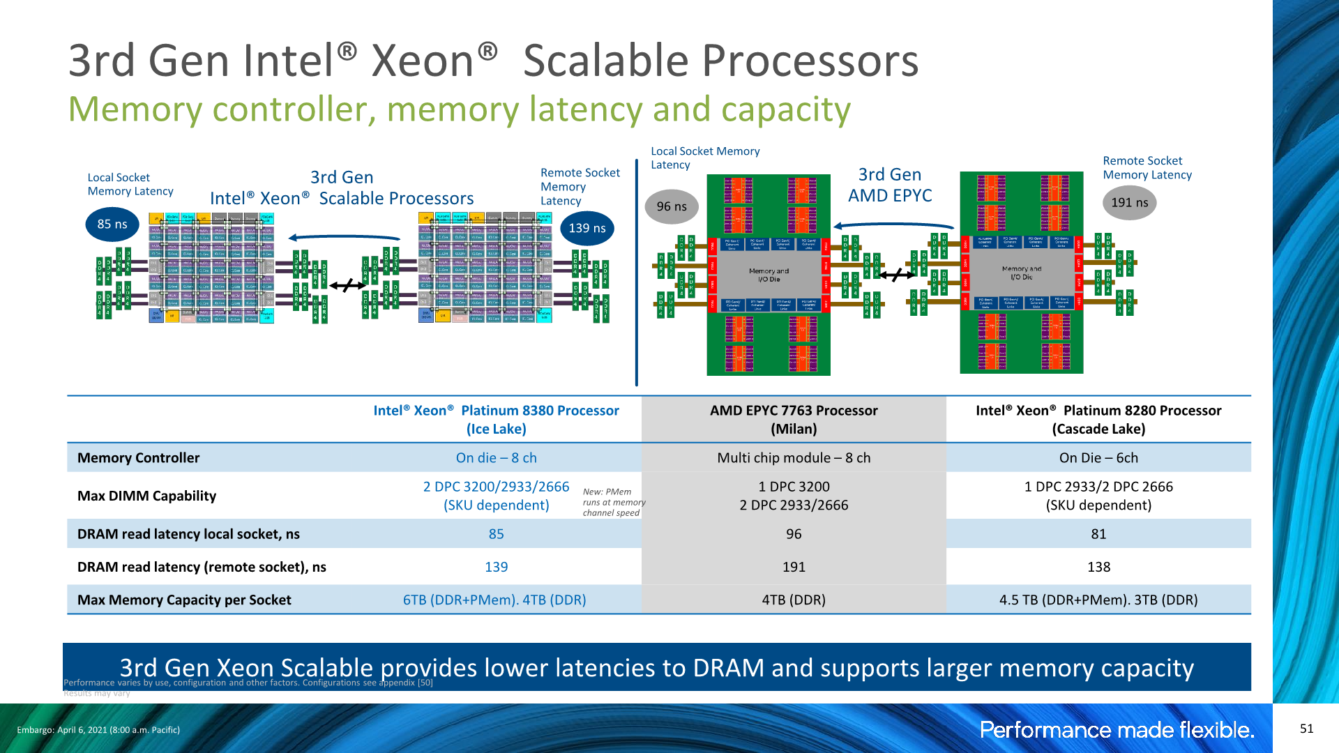
Intel’s presentations disclosed similar figures, although they’re using a different measuring methodology with MLC and simple patterns with prefetchers disabled, whereas we simply measure full random latency including TLB misses.
We weren’t able to verify the claim, but Intel also advertises advantages in remote socket DRAM latencies. The difference here matches what we’re seeing with the core-to-core latency tests, but it’s a bit of an oddball metric as I have trouble thinking of workloads where this would matter much, unless you’re running a single NUMA node across two sockets, which should be rare.
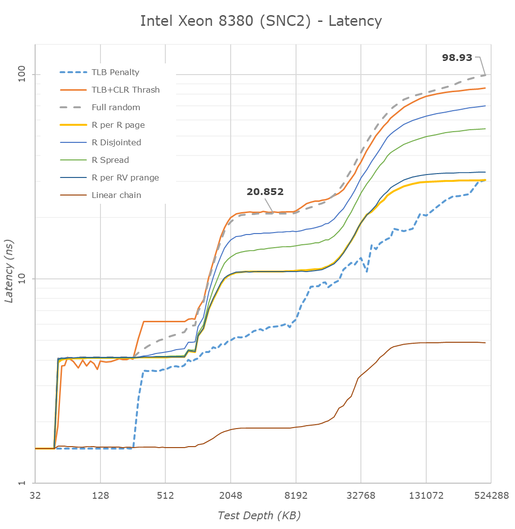
Intel had sub-NUMA clustering in prior generations, however the bigger a chip is and the larger the core count, the more these setup configurations are expected to have a difference in performance and latencies. Running the chip in SNC2 mode, meaning splitting the chip into two NUMA domains, splits the mesh into two logical parts, halving the L3 accessible to a single core, and each half only having access to their local memory controllers.
DRAM latencies here are reduced by 1.7ns, which isn’t very much a significant difference, and the L3 latencies go down by 1.2ns which is around a 5.9% reduction.
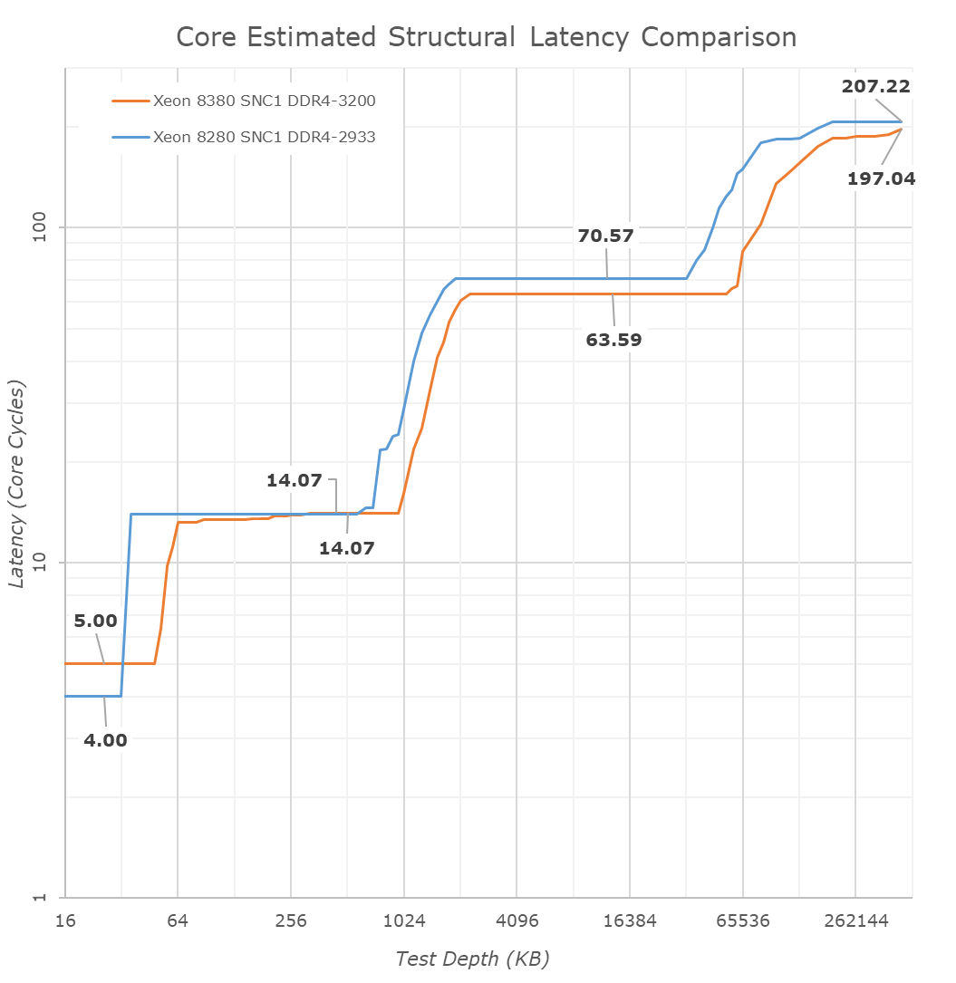
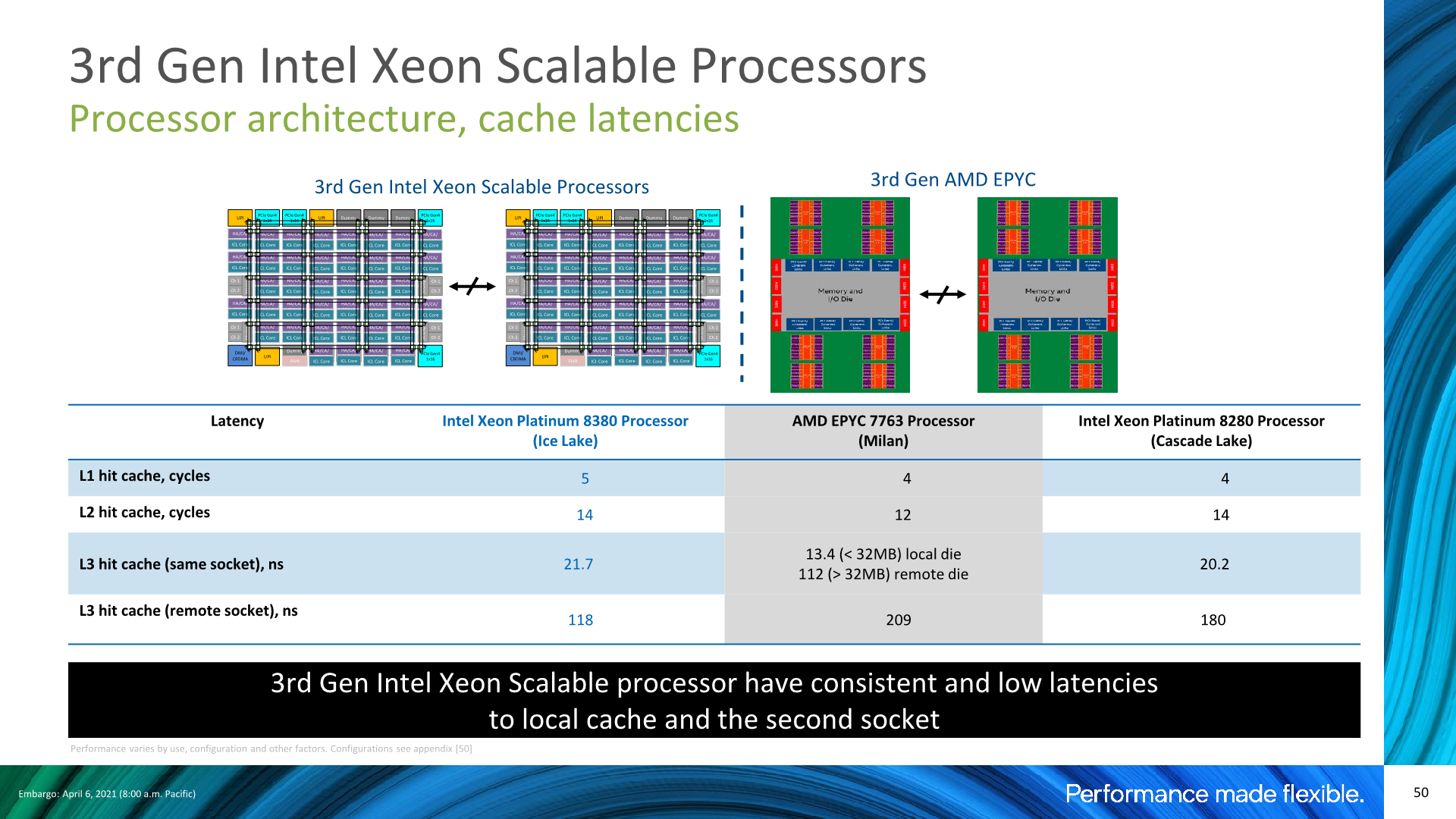
Looking at access latencies from a core cycle view, the new Ice Lake SP system is actually quite impressive. The L1 does regress from 4 to 5 cycles with the increase from 32KB to 48KB, however the L2 remains at the same 14 cycles even though it has grown from 1MB to 1.25MB.
What Intel didn’t mention in their presentation as much is that although the absolute latencies in the L3 mesh has slightly regressed from the 8280 to the new 8380, on a core clock cycle basis, it’s actually faster as we’re measuring a reduction from an average 70.5 cycles down to 63.5 cycles, which is a very impressive feat given that the mesh now contains 42% more cores, and increases its size from 38.5MB at 1.375MB/slice to 60MB at 1.5MB/slice.
Memory Bandwidth
In terms of memory bandwidth, we’re falling back to the standard STREAM benchmark, in particular the Triad test which is a simple streaming memory compute test. As I had talked about more extensively in our Ampere Altra review, I find it much more interesting to test the scaling bandwidth with increasing thread count in a system as it can reveal much more nuances of system behaviour than just a simple single figure at the arbitrary maximum thread count.
We’re also using a vanilla compilation of STREAM with GCC without any explicit optimisations that alter memory operations types, as this way it’s a more realistic representation of how most generic workloads will behave on a system.
STREAM Triad is a simple test consisting of a a[j] = b[j]+scalar*c[j]; compute kernel iterating over three memory arrays. The test assumes 3 memory operations: two memory reads and one memory write. From a hardware perspective, this can actually be 4 memory operations as many cores have to first read out a content of a target cache-line before writing to it.
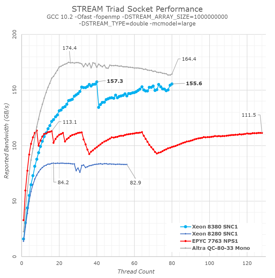
Generally, what we were expecting with Ice Lake SP were figures that were +45% ahead of Cascade Lake SP, thanks to the improved memory controllers and more memory channels. Instead, what we’re seeing here are improvements reaching up to +86%, well beyond the figures we were expecting.
As per the data, the new ICX design appears to be vastly outperforming its predecessor, and also essentially leaving AMD trailing far behind in terms of raw memory performance, only falling behind Ampere’s Altra which is able to dynamically detect streaming memory workloads and transform memory operations into non-temporal ones.
What’s also to be noted is that the per-core bandwidth this generation doesn’t seem to have improved very much from Cascade Lake SP, with AMD’s newest Milan still vastly outperforming Ice Lake SP at lower thread counts, and single-core bandwidth being much higher on the competitor systems.
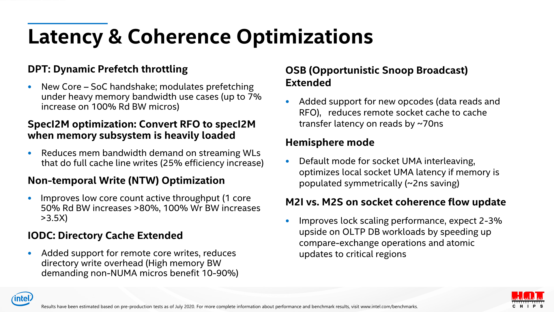
Inspecting Intel’s prior disclosures about Ice Lake SP in last year’s HotChips presentations, one point sticks out, and that is the “SpecI2M optimisation”, where the system is able to convert traditional RFO (Read for ownership) memory operations into another mechanism. We don’t know exactly what SpecI2M does, but Intel does disclose that it’s meant to optimise bandwidth and data traffic under streaming workloads. It doesn’t seem that this is a full kind of memory operation transformation into non-temporal writes as on the Arm systems we’ve seen lately, but it does significantly boost the bandwidth well beyond what we’ve seen of other x86 systems.
It’s a bit unfortunate that system vendors have ended up publishing STREAM results with hyper optimised binaries that are compiled with non-temporal instructions from the get-go, as for example we would not have seen this new mechanism on Ice Lake SP with those kind of binaries. Intel themselves are only disclosing a +47% increase in STREAM Triad performance – I consider the real-world improvement to be significantly higher than that figure, as this new dynamic mechanism doesn’t depend on specifically tuned software.
Overall, Intel’s overall larger mesh, new memory controllers, and architectural improvements in regards to memory bandwidth are absolutely impressive, and well beyond what I had expected of this generation. The latter STREAM results were really great to see as I view it as a true design innovation that will benefit a lot of workloads.


169 Comments
View All Comments
mode_13h - Monday, April 12, 2021 - link
With regard specifically to testing AVX-512, perhaps the best method is to include results both with and without it. This serves the dual-role of informing customers of the likely performance for software compiled with more typical options, as well as showing how much further performance is to be gained by using an AVX-512 optimized build.KurtL - Wednesday, April 7, 2021 - link
GCC the industry standard in real world? Maybe in that part of the world where you live, but not everywhere. It is only true in a part of the world. HPC centres have relied on icc for ages for much of the performance-critical code, though GCC is slowly catching up, at least for C and C++ but not at all for Fortran, an important language in HPC (I just read it made it back in the top-20 of most used languages after falling back to position 34 a year or so ago). In embedded systems and the non-x86-world in general, LLVM derived compilers have long been the norm. Commercial compiler vendors and CPU manufacturers are all moving to LLVM-based compilers or have been there for years already.Wilco1 - Wednesday, April 7, 2021 - link
Yes GCC is the industry standard for Linux. That's a simple fact, not something you can dispute.In HPC people are willing to use various compilers to get best performance, so it's certainly not purely ICC. And HPC isn't exclusively Intel or x86 based either. LLVM is increasing in popularity in the wider industry but it still needs to catch up to GCC in performance.
mode_13h - Wednesday, April 7, 2021 - link
GCC is the only supported compiler for building the Linux kernel, although Google is working hard to make it build with LLVM. They seem to believe it's better for security.From the benchmarks that Phoronix routinely publishes, each has its strengths and weaknesses. I think neither is a clear winner.
Wilco1 - Thursday, April 8, 2021 - link
Plus almost all distros use GCC - there is only one I know that uses LLVM. LLVM is slowly gaining popularity though.They are fairly close for general code, however recent GCC versions significantly improved vectorization, and that helps SPEC.
Wilco1 - Tuesday, April 6, 2021 - link
ICC and AMD's AOCC are SPEC trick compilers. Neither is used much in the real world since for real code they are typically slower than GCC or LLVM.Btw are you equally happy if I propose to use a compiler which replaces critical inner loops of the benchmarks with hand-optimized assembler code? It would be foolish not to take advantage of the extra performance you get only on those benchmarks...
ricebunny - Tuesday, April 6, 2021 - link
They are not SPEC tricks. You can use these compilers for any compliant C++ code that you have. In the last 10 years, the only time I didn’t use icc with Intel chips was on systems where I had no control over the sw ecosystem.Wilco1 - Tuesday, April 6, 2021 - link
They only exist because of SPEC. The latest ICC is now based on LLVM since it was falling further behind on typical code.ricebunny - Tuesday, April 6, 2021 - link
From my experience icc consistently produced better vectorized code.Anandtech again didn’t publicize the compiler flags they used to build the benchmark code. By default, gcc will not generate avx512 optimized code.
Wilco1 - Tuesday, April 6, 2021 - link
Maybe compared to old GCC/LLVM versions, but things have changed. There is now little difference between ICC and GCC when running SPEC in terms of vectorized performance. Note the amount of code that can benefit from AVX-512 is absolutely tiny, and the speedups in the real world are smaller than expected (see eg. SIMDJson results with hand-optimized AVX-512).And please read the article - the setup is clearly explained in every review: "We compile the binaries with GCC 10.2 on their respective platforms, with simple -Ofast optimisation flags and relevant architecture and machine tuning flags (-march/-mtune=Neoverse-n1 ; -march/-mtune=skylake-avx512 ; -march/-mtune=znver2 (for Zen3 as well due to GCC 10.2 not having znver3). "