Intel 3rd Gen Xeon Scalable (Ice Lake SP) Review: Generationally Big, Competitively Small
by Andrei Frumusanu on April 6, 2021 11:00 AM EST- Posted in
- Servers
- CPUs
- Intel
- Xeon
- Enterprise
- Xeon Scalable
- Ice Lake-SP
SPEC - Multi-Threaded Performance
Picking up from the power efficiency discussion, let’s dive directly into the multi-threaded SPEC results. As usual, because these are not officially submitted scores to SPEC, we’re labelling the results as “estimates” as per the SPEC rules and license.
We compile the binaries with GCC 10.2 on their respective platforms, with simple -Ofast optimisation flags and relevant architecture and machine tuning flags (-march/-mtune=Neoverse-n1 ; -march/-mtune=skylake-avx512 ; -march/-mtune=znver2 (for Zen3 as well due to GCC 10.2 not having znver3).
The new Ice Lake SP parts are using the -march/-mtune=icelake-server target. It’s to be noted that I briefly tested the system with the Skylake binaries, with little differences within margin of error.
I’m limiting the detailed comparison data to the flagship SKUs, to indicate peak performance of each platform. For that reason it’s not exactly as much an architectural comparison as it’s more of a top SKU comparison.
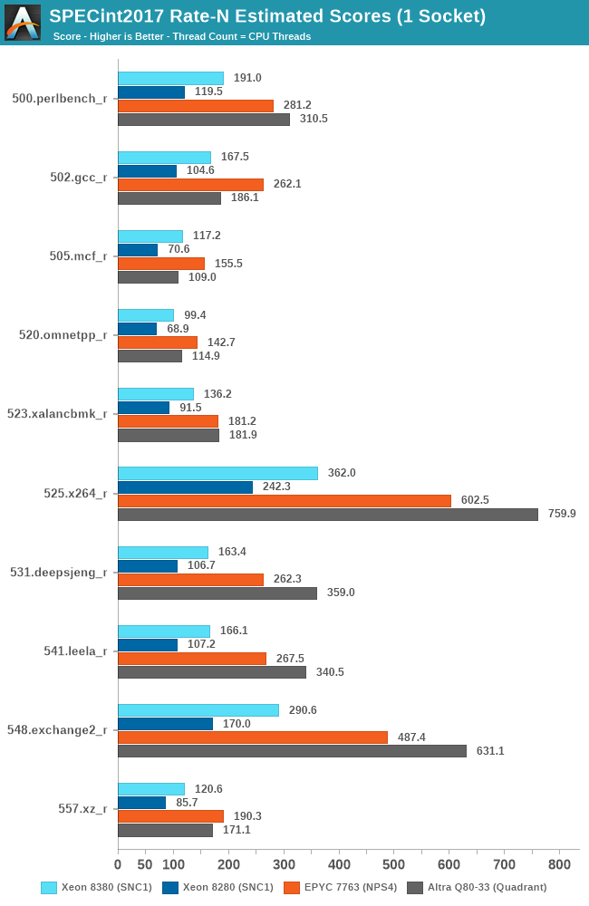
To not large surprise, the Xeon 8380 is posting very impressive performance advancements compared to the Xeon 8280, with large increases across the board for all workloads. The geo-mean increase is +54% with a low of +40% up to a high of +71%.
It’s to be noted that while the new Ice Lake system is a major generational boost, it’s nowhere near enough to catch up with the performance of the AMD Milan or Rome, or Ampere’s Altra when it comes to total throughput.
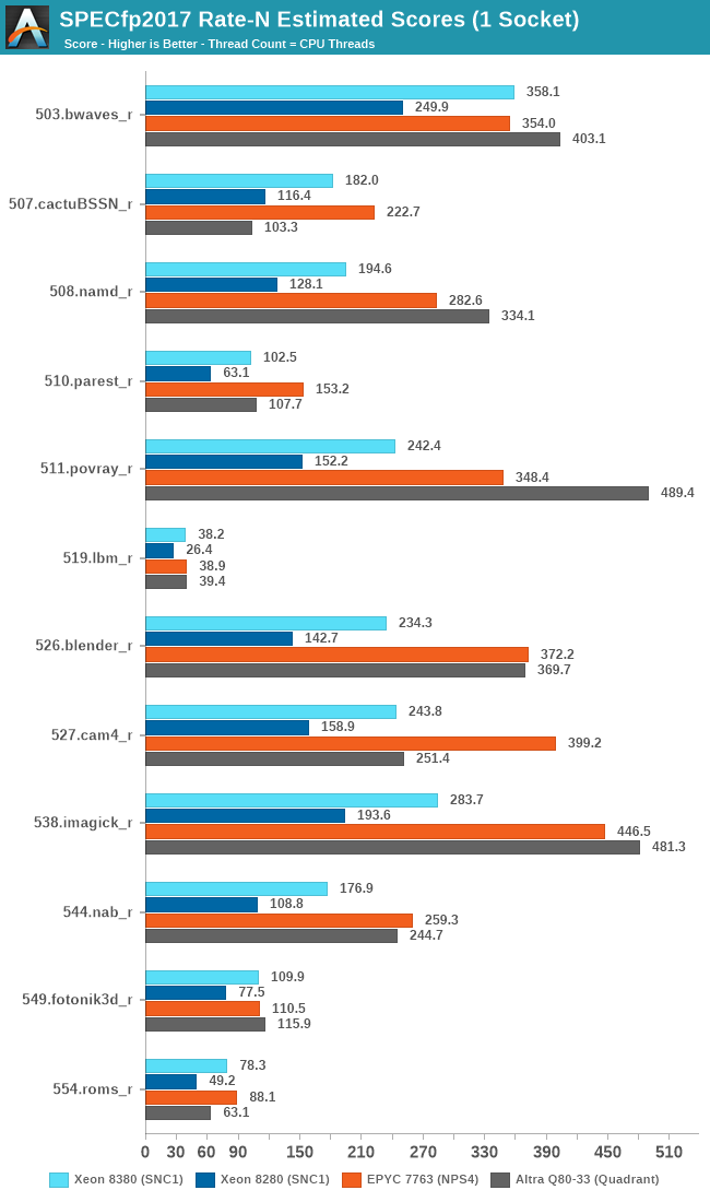
Looking at the FP suite, we have more workloads that are purely memory performance bound, and the Ice Lake Xeon 8380 again is posting significant performance increases compared to its predecessor, with a geo-mean of +53% with a range of +41% to +64%.
In some of the workloads, the new Xeon now catches up and is on par with AMD’s EPYC 7763 due to the fact that both systems have the same memory configuration with 8-channel DDR4-3200.
In any other workloads that requires more CPU compute power, the Xeon doesn’t hold up nearly as well, falling behind the competition by significant margins.
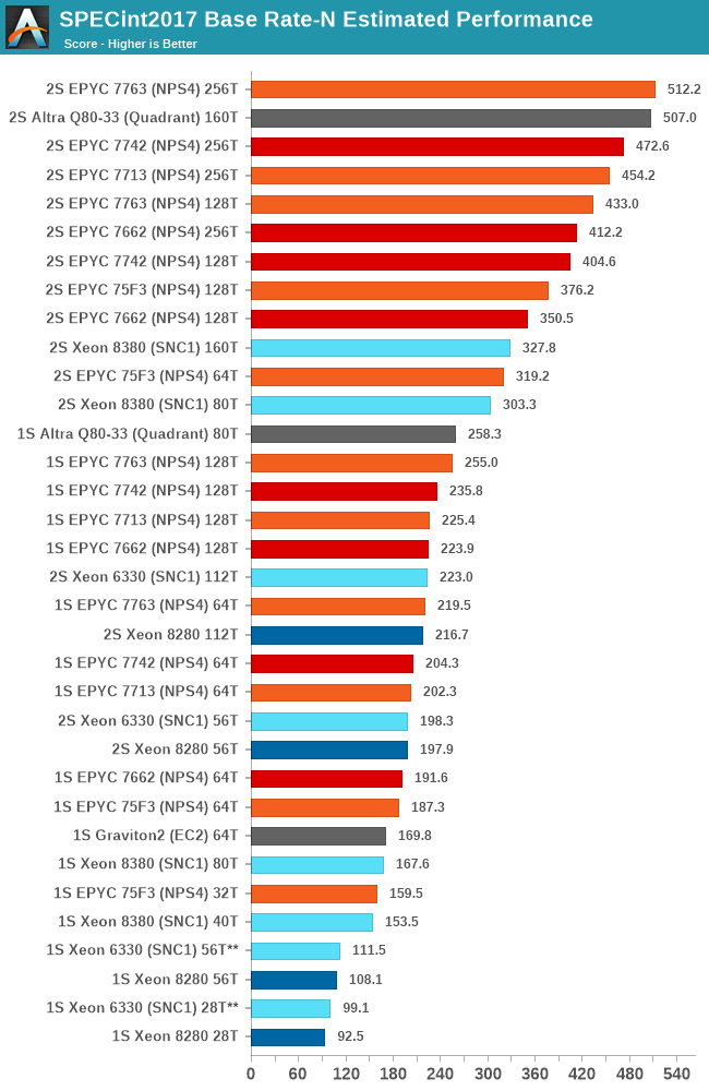
In the aggregate geomean scores, we’re seeing again that the new Xeon 8380 allows Intel to significantly reposition itself in the performance charts. Unfortunately, this is only enough to match the lower core count SKUs from the competition, as AMD and Ampere are still well ahead by massive leads – although admittedly the gap isn’t as embarrassing as it was before.
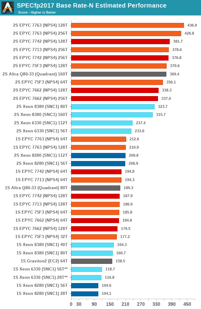
In the floating-point suite, the results are a bit more in favour for the Xeon 8380 compared to the integer suite, as the memory performance is weighed more into the total contribution of the total performance. It’s still not enough to beat the AMD and Ampere parts, but it’s much more competitive than it was before.
The Xeon 6330 is showcasing minor performance improvements over the 8280 and its cheaper equivalent the 6258R, but at least comes at half the cost – so while performance isn’t very impressive, the performance / $ might be more competitive.
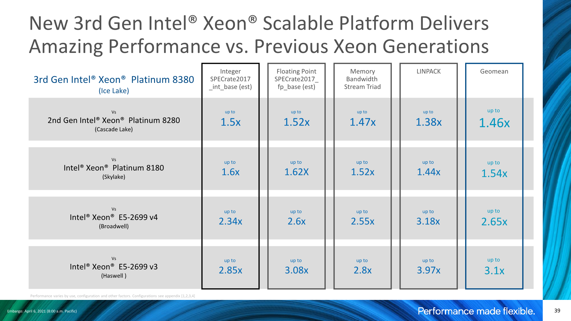
Our performance results match Intel’s own marketing materials when it comes to the generational gains, actually even surpassing Intel’s figures by a few percent.
If you would be looking at Intel’s slide above, you could be extremely enthusiastic about Intel’s new generation, as indeed the performance improvements are extremely large compared to a Cascade Lake system.
As impressive as those generational numbers are, they really only help to somewhat narrow the Grand Canyon sized competitive performance gap we’ve had to date, and the 40-core Xeon 8380 still loses out to a 32-core Milan, and from a performance / price comparison, even a premium 75F3 costs 40% less than the Xeon 8380. Lower SKUs in the Ice Lake line-up would probably fare better in perf/$, however would also just lower the performance to an even worse competitive positioning.


169 Comments
View All Comments
deil - Tuesday, April 6, 2021 - link
that's a lot of upgrade for intelGomez Addams - Tuesday, April 6, 2021 - link
That is a curious-looking wafer. I thought it was fake at first but then I noticed the alignment notch. Actually, I'm still not convinced it's real because I have seen lots and lots of wafers in various stages of production and I have never seen one where partial chips go all the way out to the edges. It's a waste of time to deal with those in the steppers so no one does that.JCB994 - Tuesday, April 6, 2021 - link
Periphery defects? I used to deal with those...buildup of material that would breakdown during wet processing and stream particles all over the wafer. Running partials as far out as possible helped. Nowadays...do they still use big wet benches? I have been out awhile...Gomez Addams - Tuesday, April 6, 2021 - link
Yes, they do. That's one of the systems I spent lots of time working on. Those don't look defects to me. They are just a continuation of the chip pattern.FullmetalTitan - Saturday, April 24, 2021 - link
Still the most chemical efficient tools for some etch processes. It is odd to see die prints out to the edge all around, usually at least the 'corners' are inked out/not patterned by the time it hits copper layers because printing features out that far can increase the chances of film delamination, which just leads to more defectivity. I suppose on DUV tools the extra few seconds to run those shots isn't THAT bad on non-immersion layers, but it adds up over timeArsenica - Tuesday, April 6, 2021 - link
It isn´t real if it doesn´t have DrIan bite marks./jk
ilt24 - Tuesday, April 6, 2021 - link
@Gomez AddamsI spent my entire career working in the semiconductor industry, although in IT, and I have seen many wafers from 4" to 12" and printing partial die off the edge of the wafer is quite common.
check out the pictures in these article:
https://www.anandtech.com/show/15380/i-ran-off-wit...
https://www.anandtech.com/show/9723/amd-to-spinoff...
Kamen Rider Blade - Tuesday, April 6, 2021 - link
So when are we going to hit 450 mm / 18" waffers?Are we ever going to get Hexagonal Die's to maximize possible Yields?
http://www.semiconductor-today.com/news_items/2020...
https://semiaccurate.com/2015/05/18/disco-makes-he...
They can already do that for simple LED's, but trying to bring Hexagonal IC Dies into existence is going to be exciting because there is a theoretical 62.5% increase in Manufactured Dies for a given Waffer Diameter and using Hexagonal IC Dies of a similar/identical area.
ilt24 - Tuesday, April 6, 2021 - link
@Kamen Rider Blade - "So when are we going to hit 450 mm / 18" waffers?"It seems the desire to move to EUV distracted TSMC, Samsung and Intel who are probably the only companies that were really interested in 450mm.
saratoga4 - Tuesday, April 6, 2021 - link
>So when are we going to hit 450 mm / 18" waffers?For logic, never since there is little to no advantage to larger wafers. Possibly NAND might use it, but we'll see if its even worth it there.
>Are we ever going to get Hexagonal Die's to maximize possible Yields?
Probably not for logic. With reticle sizes getting smaller in the coming nodes, it makes even less sense going forward then it did in the past, and it didn't make much sense then to begin with.