Intel 3rd Gen Xeon Scalable (Ice Lake SP) Review: Generationally Big, Competitively Small
by Andrei Frumusanu on April 6, 2021 11:00 AM EST- Posted in
- Servers
- CPUs
- Intel
- Xeon
- Enterprise
- Xeon Scalable
- Ice Lake-SP
SPEC - Single-Threaded Performance
Single-thread performance of server CPUs usually isn’t the most important metric for most scale-out workloads, but there are use-cases such as EDA tools which are pretty much single-thread performance bound.
Power envelopes here usually don’t matter, and what is actually the performance factor that comes at play here is simply the boost clocks of the CPUs as well as the IPC improvement, and memory latency of the cores.
The one hiccup for the Xeon 8380 this generation is the fact that although there’s plenty of IPC gains to be had compared to previous microarchitectures, the new SKU is only boosting up to 3.4GHz, whereas the 8280 was able to boost up to 4GHz, which is a 15% deficit.
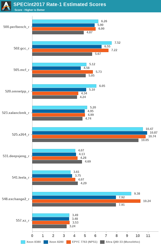
Even with the clock frequency disadvantage, thanks to the IPC gains, much improved memory bandwidth, as well as the much larger L3 cache, the new Ice Lake part to most of the time beat the Cascade Lake part, with only a couple of compute-bound core workloads where it falls behind.
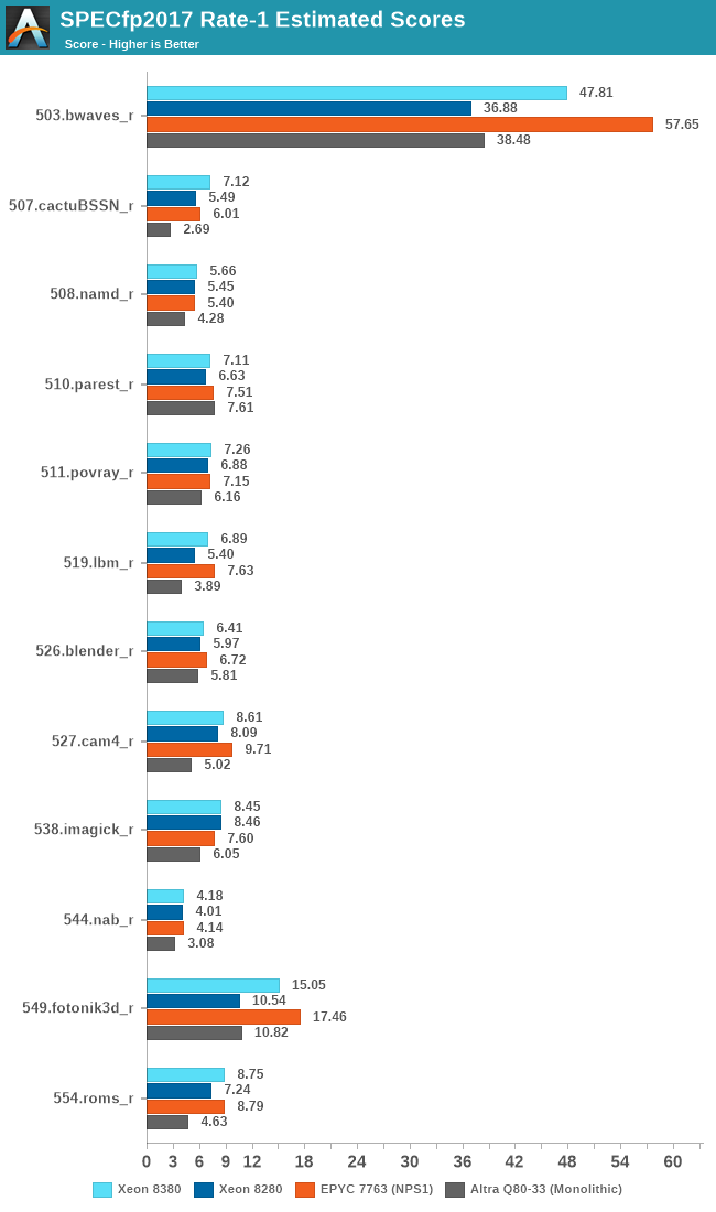
The floating-point figures are more favourable to the ICX architecture due to the stronger memory performance.
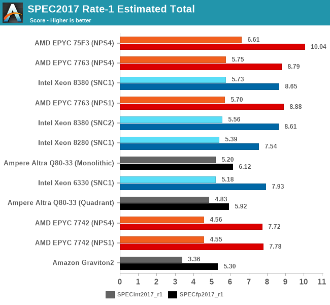
Overall, the new Xeon 8380 at least manages to post slight single-threaded performance increases this generation, with larger gains in memory-bound workloads. The 8380 is essentially on par with AMD’s 7763, and loses out to the higher frequency optimised parts.
Intel has a few SKUs which offers slightly higher ST boost clocks of up to 3.7GHz – 300Mhz / 8.8% higher than the 8380, however that part is only 8-core and features only 18MB of cache. Other SKUS offer 3.5-3.6GHz boosts, but again less cache. So while the ST figures here could improve a bit on those parts, it’s unlikely to be significant.


169 Comments
View All Comments
deil - Tuesday, April 6, 2021 - link
that's a lot of upgrade for intelGomez Addams - Tuesday, April 6, 2021 - link
That is a curious-looking wafer. I thought it was fake at first but then I noticed the alignment notch. Actually, I'm still not convinced it's real because I have seen lots and lots of wafers in various stages of production and I have never seen one where partial chips go all the way out to the edges. It's a waste of time to deal with those in the steppers so no one does that.JCB994 - Tuesday, April 6, 2021 - link
Periphery defects? I used to deal with those...buildup of material that would breakdown during wet processing and stream particles all over the wafer. Running partials as far out as possible helped. Nowadays...do they still use big wet benches? I have been out awhile...Gomez Addams - Tuesday, April 6, 2021 - link
Yes, they do. That's one of the systems I spent lots of time working on. Those don't look defects to me. They are just a continuation of the chip pattern.FullmetalTitan - Saturday, April 24, 2021 - link
Still the most chemical efficient tools for some etch processes. It is odd to see die prints out to the edge all around, usually at least the 'corners' are inked out/not patterned by the time it hits copper layers because printing features out that far can increase the chances of film delamination, which just leads to more defectivity. I suppose on DUV tools the extra few seconds to run those shots isn't THAT bad on non-immersion layers, but it adds up over timeArsenica - Tuesday, April 6, 2021 - link
It isn´t real if it doesn´t have DrIan bite marks./jk
ilt24 - Tuesday, April 6, 2021 - link
@Gomez AddamsI spent my entire career working in the semiconductor industry, although in IT, and I have seen many wafers from 4" to 12" and printing partial die off the edge of the wafer is quite common.
check out the pictures in these article:
https://www.anandtech.com/show/15380/i-ran-off-wit...
https://www.anandtech.com/show/9723/amd-to-spinoff...
Kamen Rider Blade - Tuesday, April 6, 2021 - link
So when are we going to hit 450 mm / 18" waffers?Are we ever going to get Hexagonal Die's to maximize possible Yields?
http://www.semiconductor-today.com/news_items/2020...
https://semiaccurate.com/2015/05/18/disco-makes-he...
They can already do that for simple LED's, but trying to bring Hexagonal IC Dies into existence is going to be exciting because there is a theoretical 62.5% increase in Manufactured Dies for a given Waffer Diameter and using Hexagonal IC Dies of a similar/identical area.
ilt24 - Tuesday, April 6, 2021 - link
@Kamen Rider Blade - "So when are we going to hit 450 mm / 18" waffers?"It seems the desire to move to EUV distracted TSMC, Samsung and Intel who are probably the only companies that were really interested in 450mm.
saratoga4 - Tuesday, April 6, 2021 - link
>So when are we going to hit 450 mm / 18" waffers?For logic, never since there is little to no advantage to larger wafers. Possibly NAND might use it, but we'll see if its even worth it there.
>Are we ever going to get Hexagonal Die's to maximize possible Yields?
Probably not for logic. With reticle sizes getting smaller in the coming nodes, it makes even less sense going forward then it did in the past, and it didn't make much sense then to begin with.