The Snapdragon 888 vs The Exynos 2100: Cortex-X1 & 5nm - Who Does It Better?
by Andrei Frumusanu on February 8, 2021 3:00 AM EST- Posted in
- Mobile
- Samsung
- Qualcomm
- Smartphones
- SoCs
- Snapdragon 888
- Exynos 2100
Mixed-Usage Power & Preliminary Battery Life
We haven’t had both Galaxy S21 Ultra devices long enough to do our more extensive battery life testing routines, however I did run some more power analysis on the more compute-heavy PCMark suite as well as some battery life numbers at 120Hz.
I’ll start off with some power profiling – these figures are generally within 5% margin of error accurate in terms of power usage at the battery level but are measured as input power into device as this allows us much higher resolution data sampling, without actually dismantling the phones.
I put the devices to minimum brightness to minimise screen power attribution in the power figures, with the devices set to 120Hz mode and a lamp shining on them to enable the 120Hz VRR/LFD power savings on the display. Both devices are in their default performance modes.
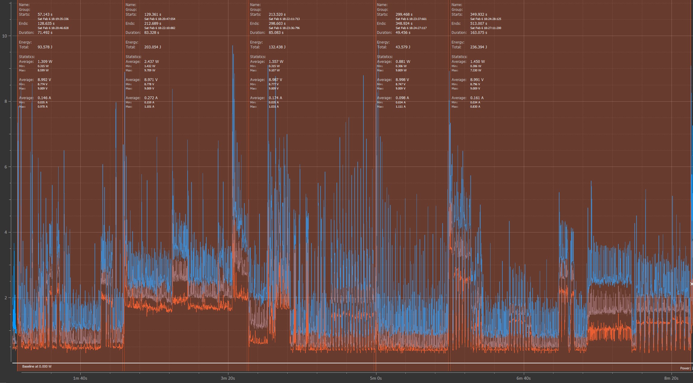
Galaxy S21 Ultra - Snapdragon 888
The Snapdragon 888’s power chart looks relatively straightforward here, with the different sections corresponding to the different sub-tests in PCMark. We see a varied amount of activity with clear activity spikes and corresponding power spikes when the SoC had to do computations.
Instantaneous peak power is around the 9W mark, which should be mostly due to the Cortex-X1 cores of the chip running alongside the Cortex-A78 cores.
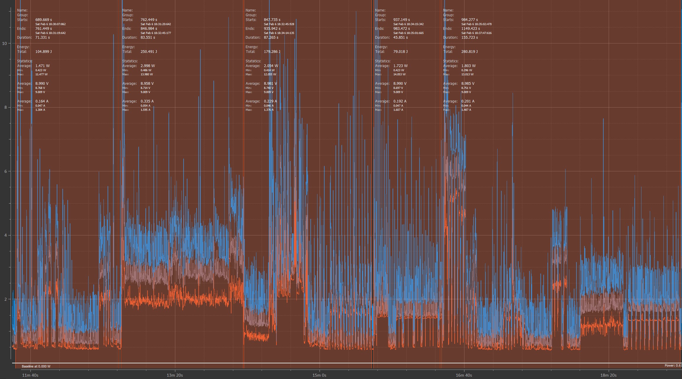
Galaxy S21 Ultra - Exynos 2100
The Exynos chart looks generally similar, which is no surprise given that it’s the same workload. What’s more interesting about the Exynos though is that it has much larger power spikes, up to 14W, which is notably more than the Snapdragon. The Cortex-A78 cores on the Exynos run much higher frequency and power than on the Snapdragon, and together with the higher power draw of the X1 cores, it makes sense that the Exynos’ instantaneous power is considerably higher when all the cores are under load.
The photo editing section of the test is very intriguing as the power profile is very different to that of the Snapdragon. This RenderScript section should be accelerated by the GPU, and here we see the Exynos’ baseline power goes up significantly compared to the Snapdragon for the majority of the test. This is almost 1W in magnitude – I really wonder what’s happening here under the hood and where that power comes from – maybe the GPU doesn’t have as fine-grained power gating or DVFS?
| Galaxy S21 Ultra Power Usage in PCMark Minimum Brightness, 120Hz, Default Performance Mode |
|||
| Snapdragon 888 Score - Power Usage |
Exynos 2100 Score - Power Usage |
% Difference Exynos vs Snapdragon |
|
| Idle Score Screen | 759mW | 797mW | +4.8% |
| Web-browsing | 12935 - 1309mW |
13159 - 1471mW |
+1.1% - +11.0% |
| Video Editing | 7866 - 2437mW |
6576 - 2998mW |
-16.4% - +18.7% |
| Writing 2.0 | 12966 - 1556mW |
15370 - 2054mW |
+18.5% - +24.2% |
| Photo Editing | 26884 - 881mW |
32385 - 1723mW |
+20.4% - +48.9% |
| Data Manipulation | 9918 - 1450mW |
8930 - 1803mW |
-10% - +19.6% |
Tabulating the PCMark test scores with the respective power figures across both Galaxy S21 Ultras, we see a few trends.
Performance wise, surprisingly enough, the Exynos has a few sub-tests where it outperforms the Snapdragon, notably in the Web-browsing, Writing and Photo editing tests. The Writing subtest particularly shows a +18% advantage in favour of the Exynos, while it loses more notably in the more single-threaded bound Data Manipulation test.
What’s also notable is that the Exynos’ power consumption is quite higher, across the board on all tests. The Photo Editing test aside where it has a 49% power disadvantage (which is actually high if we were to account for baseline device power), the rest of the test should be apples-to-apples CPU comparisons. We’re seeing roughly +15-20% device power disadvantages, and when account for baseline, this actually grows to around 18-35%. The Exynos does showcase a performance advantage in some of the tests, but not enough to make up for the increased power, meaning perf/W is lower.
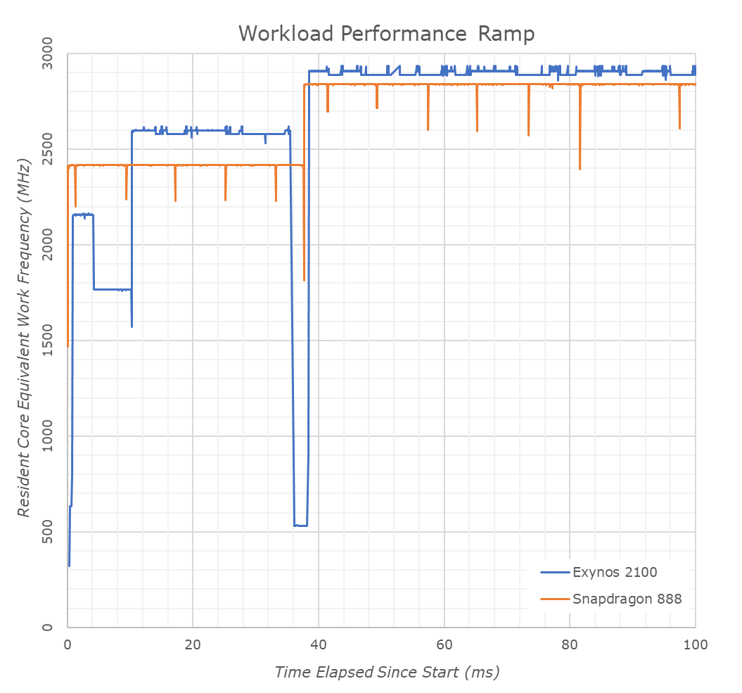
Looking at the DVFS of the two chips, we see that they’re generally reaching peak performance at roughly the same time in around 37-38ms. The Snapdragon 888 will schedule a workload directly on the A78 cores at 2.41GHz during that time before ramping up to the X1 cores at 2.84GHz. The Exynos starts off on the A55 cores at idle frequencies around 400-624MHz for 900µs, ramping up to 2210MHz for 4.2ms, before migrating onto the Cortex-A78 cores which start at 1768MHz and ramp up to 2600MHz. Oddly enough, when migrating to the X1 cores the scheduler seems to have troubles migrating the load as the cores run at the idle 533MHz before realising they have work to do and ramp up to the maximum 2.91GHz.
What’s interesting about the Exynos here is that for single-threaded workloads it doesn’t actually visit the A78’s max frequencies – which is actually a benefit for power efficiency and makes the SoC behave more like the Snapdragon counterparts even though is has higher peak frequencies. What’s a bit concerning to see is that even in this extremely simplistic load which is just an add dependency chain, the X1 cores on the Exynos don’t look solid, but rather fluctuate quite a bit. The resulting 2888MHz readout actually doesn’t exist in the SoC’s frequency tables, so I have to wonder if that’s actually real, or if Samsung has employed some new sort of hardware DFS mechanism that works on extremely fine-grained timescales.
In terms of battery life in PCMark between the two phones, because we measured higher power draw on the Exynos, we naturally also see lower battery life on the new Samsung chip compared to the Snapdragon 888 variant of the S21 Ultra. The battery life here is tested in our traditional fashion, with the screen calibrated to 200cd/m² brightness.
The Snapdragon 888 S21 Ultra here fares better than the Galaxy S20 Ultra in terms of battery life, but by a quite minor amount. These results aren’t exactly great given the S21 Ultra’s massively more advanced and more efficient display.
For the Exynos 2100 S21 Ultra, the battery results here are actually slightly worse than the Exynos 990 S20 Ultra. This means that despite the new much more efficient screen, the Exynos 2100 is so aggressive in terms of performance scaling, that it draws notably more average power than the Exynos 990. Yes, the Exynos 2100 is also significantly more performant than its predecessor and this is immediately visible in terms of device usage, but it’s performance that wasn’t just achieved through efficiency, but also through more power usage.
We also got a smaller S21 with the Exynos 2100 – this variant as well as the S21+ do not have the new super-efficient OLED screen the S21 Ultra has, and as such the SoC’s more aggressive power draw is more prominently showcased through quite bad power efficiency in this test at 120Hz.
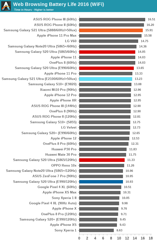
In the web-browsing test, which is less compute heavy and leans more towards display power consumption, both the new S21 Ultras fare significantly better than their predecessor due to the now much improved OLED display. These 120Hz numbers (at QHD no less), are actually fantastic, and just shows the new advancements of the new panel.
Nevertheless, the Snapdragon 888 variant of the S21 Ultra is still falling ahead of the Exynos 2100 version due to the better SoC efficiency and lower power levels. The 12.7% lead here is also similar to the general SoC efficiency differences we’ve seen in the other tests.
Update: February 14th - I'm retracting the 120Hz battery life results of the new VRR/LFD display devices pending re-testing, after discovering power-management inconsistencies in the test results. 60Hz results seem unaffected. Further details in the full review.
As we spend more times with the devices, we’ll be completing the test numbers at 60Hz as well as getting data from our web-browsing test. For the time being, the general view is that these new SoCs showcase quite increased performance, however their power draw has also gone up – meaning that battery life generationally should actually go down – with the exception of other non-SoC factors such as the S21 Ultra’s new more efficient display panel.


123 Comments
View All Comments
serendip - Monday, February 8, 2021 - link
I'm interested in what this means for the SD8cx successor. A 30% increase from using one or two X1 cores would be great, I'm using the SQ2 chip and that's fast enough for typical office tasks. That's still not enough to get within striking range of the M1 or even A14. What the heck is in those Firestorms that makes them so fast?On memory subsystems, what are Qualcomm and Samsung doing wrong compared to Apple and HiSilicon? The M1's memory bandwidth is astonishingly high but that's from using custom parts. HiSilicon is doing a great job using standard ARM interconnects.
Agreed on the stupidly high GPU clocking. The SQ2 has a beefy GPU that performs well but it can get hot even in a large tablet form factor. It's time to stop the marketing departments from forcing engineers to chase pointless metrics.
ikjadoon - Monday, February 8, 2021 - link
>What the heck is in those Firestorms that makes them so fast?A trifecta that I share with people because this question comes up so often.
Technical Part 1: https://www.anandtech.com/show/16226/apple-silicon...
Technical Part 2: https://www.anandtech.com/show/16252/mac-mini-appl...
Consumer + Approachable: https://www.youtube.com/watch?v=3SG5e4z-Ygg
Technical Background + More Approachable: https://www.youtube.com/watch?v=cAjarAgf0nI
As Upscaled wrote, "It's not magic. It's good design." And why don't AMD / Intel have these same good designs? The videos above give thorough answers. For example, the last link explains why everyone cares Firestorm (A14) and Lightning (A13) have an 8-wide decode, which is one of many major "better designs" versus competing Arm & x86 CPUs.
ikjadoon - Monday, February 8, 2021 - link
Uh, wait. Delete. I definitely skipped too much of that one. What on Earth is he going on about 1T vs 1C?~~ Consumer + Approachable: https://www.youtube.com/watch?v=3SG5e4z-Ygg ~~
Wow, I'm a little stunned at how bad this Upscaled video is. The Dev Doc + AnandTech are much more reliable.
Nicon0s - Monday, February 8, 2021 - link
LoL, Engadget.He keeps saying multithreading when he means SMT or Hyperthreading(Intel's version of SMT).
ikjadoon - Monday, February 8, 2021 - link
Yes! Never mind 1T / 1C have shown negligence IPC differences in general computing. 1% at best. Please go test an i5-8600K vs an i7-8700K: one has SMT, one does not. Terrible to see the WCCFTech disinformation cycle reach a mainstream audience so quickly.https://www.anandtech.com/show/16261/investigating...
And then he, out of left field, throws up a Cinebench multi-core score: "See? Intel and Apple are actually very close to each other." But, his comparison was the 4+4 M1 vs an 8C Intel...
I wish I could edit comments. I give up on consumer YouTube videos; I saw his earlier interview with RISC's founders and it seemed halfway decent. I'm a fool.
Archer_Legend - Tuesday, February 9, 2021 - link
Don't be offended but I think that what you posted is completely bs.First of all you are comparing arm64 cpus and x86 cpus, second the arm 64 cores used by apple are very arguably faster than the x86 cores of for example a ryzen cpu.
The second thing which I would want to point out is that about the widht of the pipeline, it is not that apple is a genious or intel and amd are stupid: the x86 architecture was built to have a narrowish pipeline and do more cycles in fact the width of the pipeline in intel and amd cpus is as wide as it gets.
Arm arch on the other end lets you use a wider pipeline, however saying using a narrower or wider pipeline is better or not is pointless because performance comes down to how you organise the cpu around that specific pipeline so....
leledumbo - Monday, February 8, 2021 - link
> What the heck is in those Firestorms that makes them so fast?The same thing since A9 again (CMIIW): super wide decoder + super big cache. Apple isn't stingy when it comes to die size and Apple SoCs are always bigger than Snapdragon on the same generation and process node. 4mm^2 difference is huge when we're talking at nm level. What's weird, Exynos is even bigger but can't match these two. No idea what Samsung put there.
Santoval - Tuesday, February 9, 2021 - link
"What's weird, Exynos is even bigger but can't match these two. No idea what Samsung put there."This is probably due to TSMC having a *far* denser 5nm process node compared to Samsung's process 5nm node. Per the article below TSMC's 5nm node tops at 173 million transistors per mm^2 while Samsung's 5nm node reaches only 126.5 MTr/mm^2 (i.e. barely denser than TSMC's second gen 7nm+ node) due to much more, er, "conservative" design choices (Samsung basically just switched from DDB cells in 7nm to SDB cells; the article explains what that means).
What is often not clear is that the quoted transistor densities of each process node are always the *maximum* transistor densities, not the actual transistor densities used to fab a die. For instance Intel have three different 10nm node variants with three different densities, a low, mid and high density variant (ranging I believe from ~55 million to ~100 million transistors per mm^2). The last one is the only one that has been widely reported, the other two were intended for the tech savvy press and audience.
Each Intel 10nm die has a mix of all three libraries, but each design is (obviously) *fixed* with a precise mix of the three. The desktop parts always have a higher percentage of low density cells because these need to clock higher, and vice versa for the mobile parts. Mobile phones are efficiency focused, so their SoCs have the highest percentage of the highest density variant of each process node that is possible (without hindering performance too much).
That is an additional reason their clocks top at ~3 GHz. Since the two SoCs of the article are both mobile SoCs of an almost identical design we can assume a roughly equivalent percentage of the highest density cells each process node maxes out at. Thus, if all else was being equal (including the same iGPU) Samsung's SoC would have a roughly ~27% larger die than TSMC's SoC. That must be the main reason Samsung kept the cache sizes of the X1 and the A55 cores low.
Santoval - Tuesday, February 9, 2021 - link
p.s. Sorry, I forgot the link to the article :https://semiwiki.com/semiconductor-manufacturers/s...
Santoval - Tuesday, February 9, 2021 - link
p.s.2 I just noticed that the Snapdragon 888 is also fabbed with Samsung's 5nm node. While that rendered the comparison between the two SoCs in my above comment moot the other things I pointed out might have some "academic" value regarding process nodes (I have no away to delete the comment anyway..).