Apple Announces The Apple Silicon M1: Ditching x86 - What to Expect, Based on A14
by Andrei Frumusanu on November 10, 2020 3:00 PM EST- Posted in
- Apple
- Apple A14
- Apple Silicon
- Apple M1
Dominating Mobile Performance
Before we dig deeper into the x86 vs Apple Silicon debate, it would be useful to look into more detail how the A14 Firestorm cores have improved upon the A13 Lightning cores, as well as detail the power and power efficiency improvements of the new chip’s 5nm process node.
The process node is actually quite the wildcard in the comparisons here as the A14 is the first 5nm chipset on the market, closely followed by Huawei’s Kirin 9000 in the Mate 40 series. We happen to have both devices and chips in house for testing, and contrasting the Kirin 9000 (Cortex-A77 3.13GHz on N5) vs the Snapdragon 865+ (Cortex-A77 3.09GHz on N7P) we can somewhat deduct how much of an impact the process node has in terms of power and efficiency, translating those improvements to the A13 vs A14 comparison.

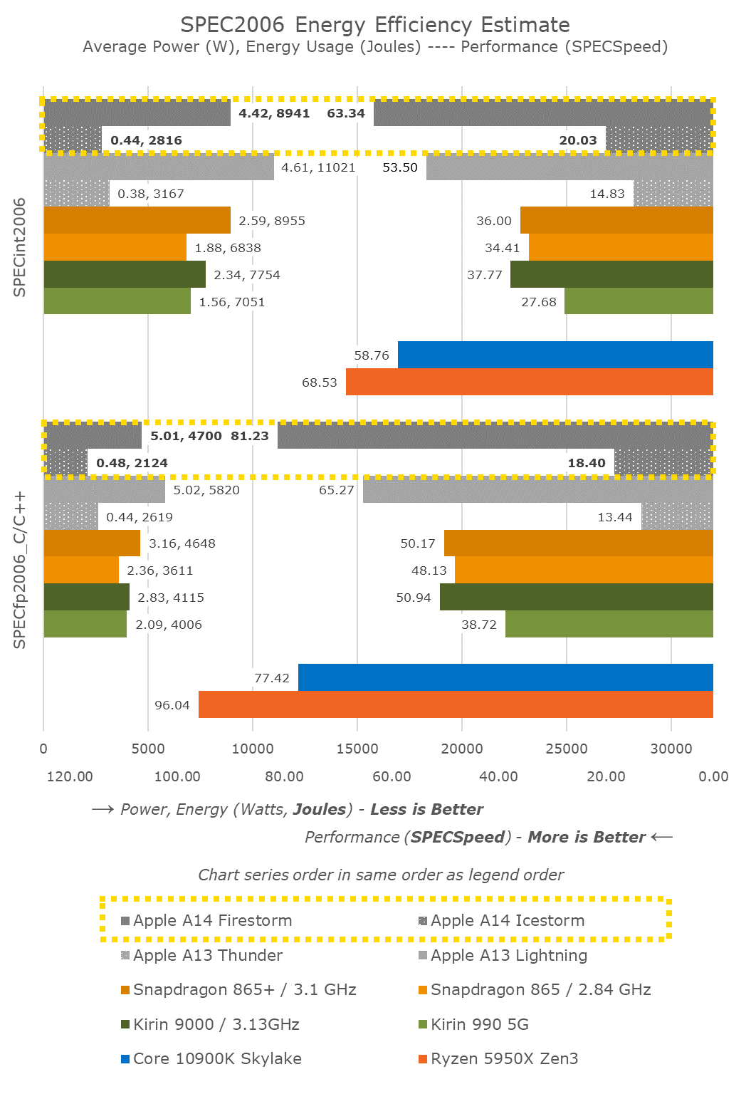
Starting off with SPECint2006, we don’t see anything very unusual about the A14 scores, save the great improvement in 456.hmmer. Actually, this wasn’t due to a microarchitectural jump, but rather due to new optimisations on the part of the new LLVM version in Xcode 12. It seems here that the compiler has employed a similar loop optimisation as found on GCC8 onwards. The A13 score actually had improved from 47.79 to 64.87, but I hadn’t run new numbers on the whole suite yet.
For the rest of the workloads, the A14 generally looks like a relatively linear progression from the A13 in terms of progression, accounting for the clock frequency increase from 2.66GHz to 3GHz. The overall IPC gains for the suite look to be around 5% which is a bit less than Apple’s prior generations, though with a larger than usual clock speed increase.
Power consumption for the new chip is actually in line, and sometimes even better than the A13, which means that workload energy efficiency this generation has seen a noticeable improvement even at the peak performance point.
Performance against the contemporary Android and Cortex-core powered SoCs looks to be quite lopsided in favour of Apple. The one thing that stands out the most are the memory-intensive, sparse memory characterised workloads such as 429.mcf and 471.omnetpp where the Apple design features well over twice the performance, even though all the chip is running similar mobile-grade LPDDR4X/LPDDR5 memory. In our microarchitectural investigations we’ve seen signs of “memory magic” on Apple’s designs, where we might believe they’re using some sort of pointer-chase prefetching mechanism.
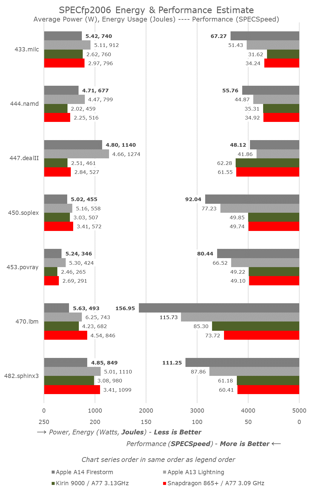
In SPECfp, the increases of the A14 over the A13 are a little higher than the linear clock frequency increase, as we’re measuring an overall 10-11% IPC uplift here. This isn’t too surprising given the additional fourth FP/SIMD pipeline of the design, whereas the integer side of the core has remained relatively unchanged compared to the A13.
In the overall mobile comparison, we can see that the new A14 has made robust progress in terms of increasing performance over the A13. Compared to the competition, Apple is well ahead of the pack – we’ll have to wait for next year’s Cortex-X1 devices to see the gap narrow again.
What’s also very important to note here is that Apple has achieved this all whilst remaining flat, or even lowering the power consumption of the new chip, notably reducing energy consumption for the same workloads.
Looking at the Kirin 9000 vs the Snapdragon 865+, we’re seeing a 10% reduction in power at relatively similar performance. Both chips use the same CPU IP, only differing in their process node and implementations. It seems Apple’s A14 here has been able to achieve better figures than just the process node improvement, which is expected given that it’s a new microarchitecture design as well.
One further note is the data of the A14’s small efficiency cores. This generation we saw a large microarchitectural boost on the part of these new cores which are now seeing 35% better performance versus last year’s A13 efficiency cores – all while further reducing energy consumption. I don’t know how the small cores will come into play on Apple’s “Apple Silicon” Mac designs, but they’re certainly still very performant and extremely efficient compared to other current contemporary Arm designs.
Lastly, there’s the x86 vs Apple performance comparison. Usually for iPhone reviews I comment on this in this section of the article, but given today’s context and the goals Apple has made for Apple Silicon, let’s investigate that into a whole dedicated section…


644 Comments
View All Comments
mdriftmeyer - Thursday, November 12, 2020 - link
Logic Pro Xvais - Thursday, November 12, 2020 - link
Great article until it reached the benchmark against x86 part.I am amazed how something can claim to be a benchmark and yet leave out what is being measured, what are the criteria, are the results adjusted for power, etc.
Here are some quotes from the article and why they seem to be a biased towards Apple, bordering on fanboyism:
"x86 CPUs today still only feature a 4-wide decoder designs (Intel is 1+4) that is seemingly limited from going wider at this point in time due to the ISA’s inherent variable instruction length nature, making designing decoders that are able to deal with aspect of the architecture more difficult compared to the ARM ISA’s fixed-length instructions"
And who ever said wider is always better, especially in two different instruction sets? Comparing apples to melons here...
"On the ARM side of things, Samsung’s designs had been 6-wide from the M3 onwards, whilst Arm’s own Cortex cores had been steadily going wider with each generation, currently 4-wide in currently available silicon"
Based on that alone would you conclude Exynos is some miracle of CPU design and it somehow comes anywhere close to the performance of a full blown desktop enthusiast grade CPU? Sure hope not.
"outstanding lode/store:
To not surprise, this is also again deeper than any other microarchitecture on the market. Interesting comparisons are AMD’s Zen3 at 44/64 loads & stores, and Intel’s Sunny Cove at 128/72. "
Again comparing different things and drawing conclusions like it's a linear scale. AMD's load/stores are significantly less than Intel's and yes AMD Zen3 CPUs outperform Intel counterparts across the board. I'd say biased as hell...
"AMD also wouldn’t be looking good if not for the recently released Zen3 design."
So comparing yet unreleased core to the latest already available from the competition and somehow the competition is in a bad place as "only" it's latest product is better? Come on...
"The fact that Apple is able to achieve this in a total device power consumption of 5W including the SoC, DRAM, and regulators, versus +21W (1185G7) and 49W (5950X) package power figures, without DRAM or regulation, is absolutely mind-blowing."
I am really interested where those power package figures come from, specifically for the 5950X. AMD's site lists it as 105W TDP. How were the 49W measured?
I've read other articles from Andrei which have been technical, detailed and specific marvels, but this one misses the mark by a long shot in the benchmarks and conclusion parts.
Bluetooth - Thursday, November 12, 2020 - link
They don’t have an actual M1 to test as they say in the artcle. The M1 will be available on the 24th.GeoffreyA - Thursday, November 12, 2020 - link
I think it would be instructive to remember the Pentium 4, which had a lot of "fast" terms for its time: hyper-pipelined this, double pumped ALUs, quad pumped that; but we all know the result. The proof of the pudding is in the eating, or in the field of CPUs, performance, power, and silicon area.AMD and Intel have settled down to 4- and 5-wide decode as the best trade-offs for their designs. They could make it 8-wide tomorrow, but it's likely no use, and would cause disaster from a power point of view.* If Apple wishes to go for wide, good for them, but the CPU will be judged not on "I've got this and that," but on what its final merits.
Personally, I think it's better engineering to produce a good result with fewer ingredients. Compare Z3's somewhat conservative out-of-order structures to Sunny Cove's, but beating it.
When the M1 is on an equal benchmark field with 5 nm x86, then we'll see whether it's got the goods or not.
* Decoding takes up a lot of power in x86, that's why the micro-op cache is so effective (removing fetch and pre/decode). In x86, decoding can't be done in parallel, owing to the varying instruction lengths: one has to determine first how long one instruction is before knowing where the next one starts, whereas in fixed-length ISAs, like ARM, it can be done in parallel: length being fixed, we know where each instruction starts.
Joe Guide - Thursday, November 12, 2020 - link
The benchmarks are coming out, and it looks like the pudding is quite tasty. But you have a good point. When in 2025 or 2026 Intel or AMD releases their newest 5 nm x86, you will be proven to be prophetic that the new Intel chip resoundingly beats the base M1 chip from 5 years ago.GeoffreyA - Thursday, November 12, 2020 - link
That line about the M1 and 5 nm is silly on my part, I'll admit. Sometimes we write things and regret it later. Also, if you look at my comment from the other day, you'll see the first thing I did was acknowledge Apple's impressive work on this CPU. The part about the Pentium 4 and the pudding wasn't in response to the A14's performance, but this whole debate running through the comments about wide vs. narrow, and so I meant, "Wide, narrow, doesn't mean anything. What matters is the final performance."I think what I've been trying to say, quite feebly, through the comments is: "Yes, the A14 has excellent performance/watt, and am shocked how 5W can go up against 105W Ryzen. But, fanboy comment it may be, I'm confident AMD and Intel (or AMD at any rate) can improve their stuff and beat Apple."
Joe Guide - Thursday, November 12, 2020 - link
I see this as glass half full. There was been far too much complacency in the CPU development over the last decade. If it take Apple to kick the industry in the butt, well then, how is that bad.Moore's Law has awoke after a deep slumber and it is hungry and angry. Run Intel. Run for your life.
GeoffreyA - Friday, November 13, 2020 - link
Agreed, when AMD was struggling, Intel's improvements were quite meagre (Sandy Bridge excepted). Much credit must be given to AMD though. Their execution of the past few years has been brilliant.chlamchowder - Friday, November 13, 2020 - link
In x86, decoding is very much done in parallel. That's how you get 3/4/5-wide decoders. The brute force method is to tentatively start decoding at every byte. Alternatively, you mark instruction boundaries in the instruction cache (Goldmont/Tremont do this, as well as older AMD CPUs like Phenom).GeoffreyA - Saturday, November 14, 2020 - link
Thanks for that. I'm only a layman in all this, so I don't know the exact details. I did suspect there was some sort of trick going on to decode more than one at a time. Marking instructions boundaries in the cache is quite interesting because it ought to tone down, or even eliminate, x86's variable length troubles. Didn't know about Tremont and Goldmont, but I was reading that the Pentium MMX, as well as K8 to Bulldozer, perhaps K7 too, used this trick.My question is, do you think AMD and Intel could re-introduce it (while keeping the micro-op cache as well)? Is it effective or does it take too much effort itself? I ask because if it's worth it, it could help x86's length problem quite a bit, and that's something which excites me, under this current climate of ARM. However, judging from the results, it didn't aid the Athlon, Phenom, and Bulldozer that drastically, and AMD abandoned it in Zen, going for a micro-op cache instead, so that knocks down my hopes a bit.