AMD Zen 3 Ryzen Deep Dive Review: 5950X, 5900X, 5800X and 5600X Tested
by Dr. Ian Cutress on November 5, 2020 9:01 AM ESTSection by Andrei Frumusanu
Core-to-Core Latency
As the core count of modern CPUs is growing, we are reaching a time when the time to access each core from a different core is no longer a constant. Even before the advent of heterogeneous SoC designs, processors built on large rings or meshes can have different latencies to access the nearest core compared to the furthest core. This rings true especially in multi-socket server environments.
But modern CPUs, even desktop and consumer CPUs, can have variable access latency to get to another core. For example, in the first generation Threadripper CPUs, we had four chips on the package, each with 8 threads, and each with a different core-to-core latency depending on if it was on-die or off-die. This gets more complex with products like Lakefield, which has two different communication buses depending on which core is talking to which.
If you are a regular reader of AnandTech’s CPU reviews, you will recognize our Core-to-Core latency test. It’s a great way to show exactly how groups of cores are laid out on the silicon. This is a custom in-house test, and we know there are competing tests out there, but we feel ours is the most accurate to how quick an access between two cores can happen.
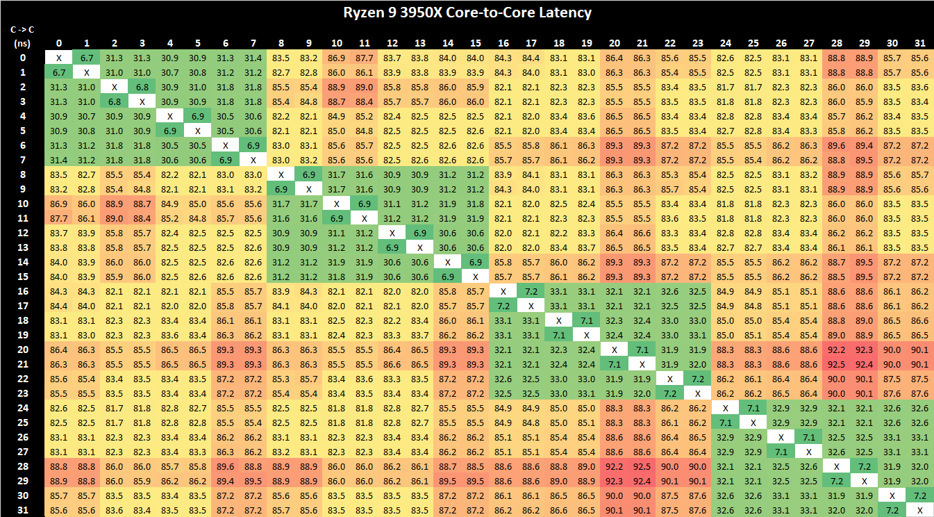
We had noted some differences in the core-to-core latency behaviour of various Zen2 CPUs depending on which motherboard and which AGESA version was tested at the time. For example, in this current version we’re seeing inter-core latencies within the L3 caches of the CCX’s falling in at around 30-31ns, however in the past we had measured on the same CPU figures in the 17ns range. We had measured a similar figure on our Zen2 Renoir tests, so it’s all the more odd to now get a 31ns figure on the 3950X while on a different motherboard. We had reached out to AMD about this odd discrepancy but never really got a proper response as to what exactly is happening here – it’s after all the same CPU and even the same test binary, just differing motherboard platforms and AGESA versions.
Nevertheless, in the result we can clearly see the low-latencies of the four CCXs, with inter-core latencies between CPUs of differing CCXs suffering to a greater degree in the 82ns range, which remains one of the key disadvantages of AMD’s core complex and chiplet architecture.
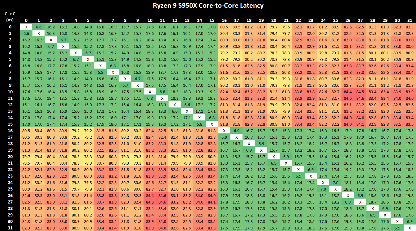
On the new Zen3-based Ryzen 9 5950X, what immediately is obvious is that instead of four low-latency CPU clusters, there are now only two of them. This corresponds to AMD’s switch from four CCX’s for their 16-core predecessor, to only two such units on the new part, with the new CCX basically being the whole CCD this time around.
Inter-core latencies within the L3 lie in at 15-19ns, depending on the core pair. One aspect affecting the figures here are also the boost frequencies of that the core pairs can reach as we’re not fixing the chip to a set frequency. This is a large improvement in terms of latency over the 3950X, but given that in some firmware combinations, as well as on AMD’s Renoir mobile chip this is the expected normal latency behaviour, it doesn’t look that the new Zen3 part improves much in that regard, other than obviously of course enabling this latency over a greater pool of 8 cores within the CCD.
Inter-core latencies between cores in different CCDs still incurs a larger latency penalty of 79-80ns, which is somewhat to be expected as the new Ryzen 5000 parts don’t change the IOD design compared to the predecessor, and traffic would still have to go through the infinity fabric on it.
For workloads which are synchronisation heavy and are multi-threaded up to 8 primary threads, this is a great win for the new Zen3 CCD and L3 design. AMD’s new L3 complex in fact now offers better inter-core latencies and a flatter topology than Intel’s ring-based consumer designs, with SKUs such as the 10900K varying between 16.5-23ns inter-core latency. AMD still has a way to go to reduce inter-CCD latency, but maybe that something to address in the next generation design.
Cache and Memory Latency
As Zen3 makes some big changes in the memory cache hierarchy department, we’re also expecting this to materialise in quite different behaviour in our cache and memory latency tests. On paper, the L1D and L2 caches on Zen3 shouldn’t see any differences when compared to Zen2 as both share the same size and cycle latencies – however we did point out in our microarchitecture deep dive that AMD did make some changes to the behaviour here due to the prefetchers as well as cache replacement policy.
On the L3 side, we expect a large shift of the latency curve into deeper memory regions given that a single core now has access to the full 32MB, double that of the previous generation. Deeper into DRAM, AMD actually hasn’t talked much at all about how memory latency would be affected by the new microarchitecture – we don’t expect large changes here due to the fact that the new chips are reusing the same I/O die with the same memory controllers and infinity fabric. Any latency effects here should be solely due to the microarchitectural changes made on the actual CPUs and the core-complex die.
Starting off in the L1D region of the new Zen3 5950X top CPU, we’re seeing access latencies of 0.792ns which corresponds to a 4-cycle access at exactly 5050MHz, which is the maximum frequency at which this new part boosts to in single-threaded workloads.
Entering the L2 region, we however are already starting to see some very different microarchitectural behaviour on the part of the latency tests as they look nothing like we’ve seen on Zen2 and prior generations.
Starting off with the most basic access pattern, a simple linear chain within the address space, we’re seeing access latencies improve from an average of 5.33 cycles on Zen2 to +-4.25 cycles on Zen3, meaning that this generation’s adjacent-line prefetchers are much more aggressive in pulling data into the L1D. This is actually now even more aggressive than Intel’s cores, which have an average access latency of 5.11 cycles for the same pattern within their L2 region.
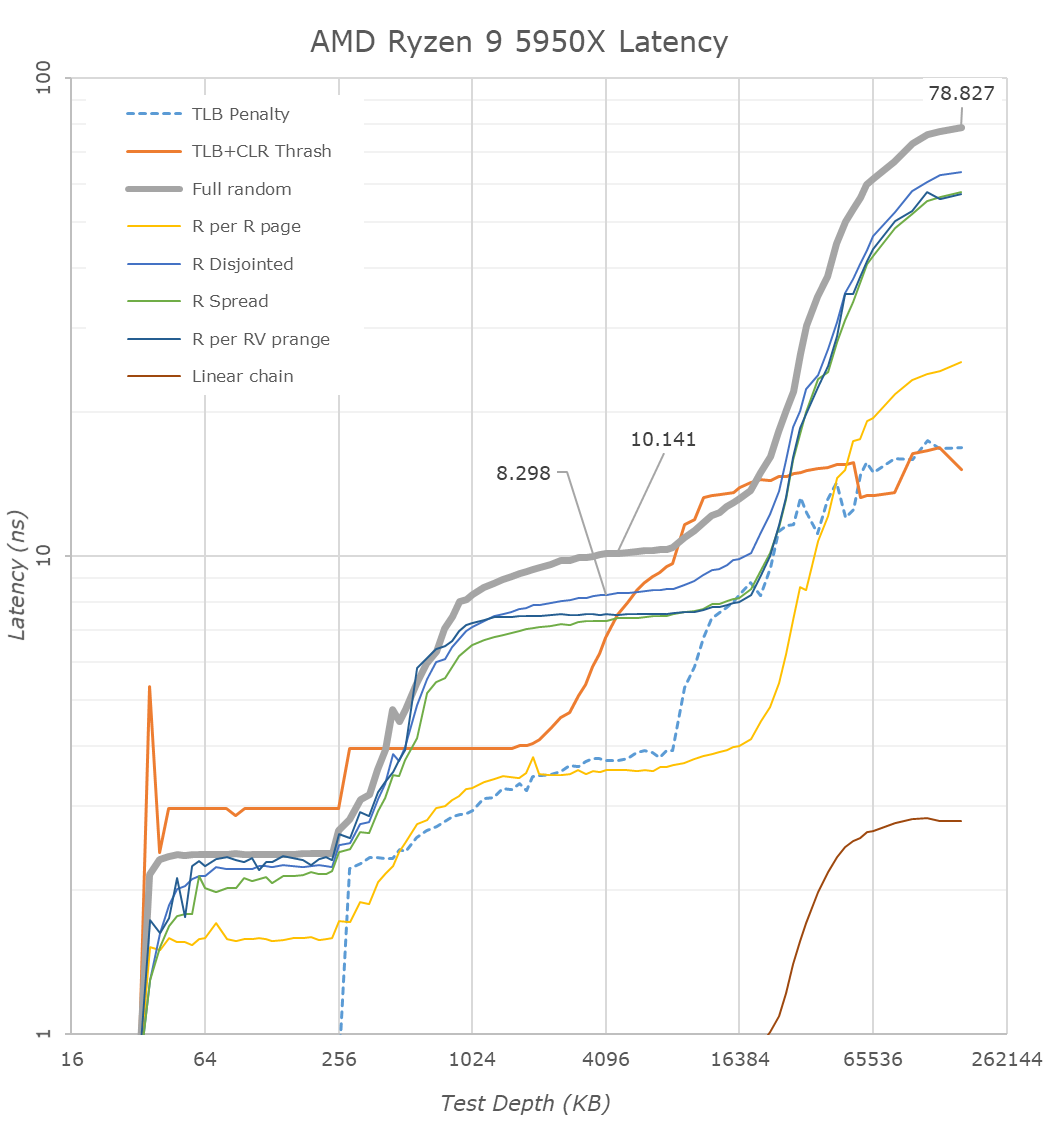
Besides the simple linear chain, we also see very different behaviour in a lot of the other patterns, some of our other more abstract patterns aren’t getting prefetched as aggressively as on Zen2, more on that later. More interestingly is the behaviour of the full random access and the TLB+CLR trash pattern which are now completely different: The full random curve is now a lot more abrupt on the L1 to L2 boundary, and we’re seeing the TLB+CLR having an odd (reproducible) spike here as well. The TLB+CLR pattern goes through random pages always hitting only a single, but every time different cache line within each page, forcing a TLB read (or miss) as well as a cache line replacement.
The fact that this test now behaves completely different throughout the L2 to L3 and DRAM compared to Zen2 means that AMD is now employing a very different cache line replacement policy on Zen3. The test’s curve in the L3 no longer actually matching the cache’s size means that AMD is now optimising the replacement policy to reorder/move around cache lines within the sets to reduce unneeded replacements within the cache hierarchies. In this case it’s a very interesting behaviour that we hadn’t seen to this degree in any microarchitecture and basically breaks our TLB+CLR test which we previously relied on for estimating the physical structural latencies of the designs.
It’s this new cache replacement policy which I think is cause for the more smoothed out curves when transitioning between the L2 and L3 caches as well as from the L3 to DRAM – the latter behaviour which now looks closer to what Intel and some other competing microarchitectures have recently exhibited.
Within the L3, things are a bit difficult to measure as there’s now several different effects at play. The prefetchers on Zen3 don’t seem to be as aggressive on some of our patterns which is why the latency here has gone up more a little bit more of a notable amount – we can’t really use them for apples-to-apples comparisons to Zen2 because they’re no longer doing the same thing. Our CLR+TLB test also not working as intended means that we’ll have to resort to full random figures; the new Zen3 cache at 4MB depth here measured in at 10.127ns on the 5950X, compared to 9.237ns on the 3950X. Translating this into cycles corresponds to a regression from 42.9 cycles to 51.1 cycles on average, or basically +8 cycles. AMD’s official figures here are 39 cycles and 46 cycles for Zen2 and Zen3, a +7-cycle regression – in line with what we measure, accounting for TLB effects.
Latencies past 8MB still go up even though the L3 is 32MB deep, and that’s simply because it exceeds the L2 TLB capacity of 2K pages with a 4K page size.
In the DRAM region, we’re measuring 78.8ns on the 5950X versus 86.0ns on the 3950X. Converting this into cycles actually ends up with an identical 398 cycles for both chips at 160MB full random-access depth. We have to note that because of that change in the cache line replacement policy that latencies appear to be better for the new Zen3 chip at test depths between 32-128MB, but that’s just a measurement side-effect and does not seem to be an actual representation of the physical and structural latency of the new chip. You’d have to test deeper DRAM regions to get accurate figures – all of which makes sense given that the new Ryzen 5000 chips are using the same I/O die and memory controllers, and we’re testing identical memory at the same 3200MHz speed.
Overall, although Zen3 doesn’t change dramatically in its cache structure beyond the doubled up and slightly slower L3, the actual cache behaviour between microarchitecture generations has changed quite a lot for AMD. The new Zen3 design seems to make much smarter use of prefetching as well as cache line handling – some of whose performance effects could easily overshadow just the L3 increase. We inquired AMD’s Mike Clarke about some of these new mechanisms, but the company wouldn’t comment on some of the new technologies that they would rather keep closer to their chest for the time being.
Frequency Ramping
Both AMD and Intel over the past few years have introduced features to their processors that speed up the time from when a CPU moves from idle into a high powered state. The effect of this means that users can get peak performance quicker, but the biggest knock-on effect for this is with battery life in mobile devices, especially if a system can turbo up quick and turbo down quick, ensuring that it stays in the lowest and most efficient power state for as long as possible.
Intel’s technology is called SpeedShift, although SpeedShift was not enabled until Skylake.
One of the issues though with this technology is that sometimes the adjustments in frequency can be so fast, software cannot detect them. If the frequency is changing on the order of microseconds, but your software is only probing frequency in milliseconds (or seconds), then quick changes will be missed. Not only that, as an observer probing the frequency, you could be affecting the actual turbo performance. When the CPU is changing frequency, it essentially has to pause all compute while it aligns the frequency rate of the whole core.
We wrote an extensive review analysis piece on this, called ‘Reaching for Turbo: Aligning Perception with AMD’s Frequency Metrics’, due to an issue where users were not observing the peak turbo speeds for AMD’s processors.
We got around the issue by making the frequency probing the workload causing the turbo. The software is able to detect frequency adjustments on a microsecond scale, so we can see how well a system can get to those boost frequencies. Our Frequency Ramp tool has already been in use in a number of reviews.
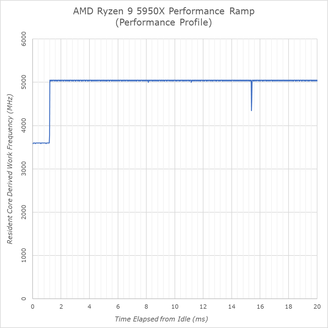
On the performance profile, the new 5950X looks to behave identical to the Ryzen 3000 series, ramping up to maximum frequency in 1.2ms. On the balanced profile, this is at 18ms to avoid needlessly upping the frequency from idle during sporadic background tasks.
Idle frequency on the new CPU lands in at 3597MHz and the Zen3 CPU here will boost up to 5050MHz on single-threaded workloads. In our test tool it actually reads out fluctuations between 5025 and 5050MHz, however that just seems to be an aliasing issue due to the timer resolution being 100ns and us measuring 20µs workload chunks. The real frequency as per base-clock and multiplier looks to be 5048.82MHz on this particular motherboard.


339 Comments
View All Comments
TheinsanegamerN - Tuesday, November 10, 2020 - link
However AMD's boost algorithim is very temperature sensitive. Those coolers may work fine, but if they get to the 70C range you're losing max performance to higher temperatures.Andrew LB - Sunday, December 13, 2020 - link
Blah blah....Ryzen 5800x @ 3.6-4.7ghz : 219w and 82'c.
Ryzen 5800x @ 4.7ghz locked: 231w and 88'c.
Fractal Celsius+ S28 Prisma 280mm AIO CPU cooler at full fan and pump speed
https://www.kitguru.net/components/cpu/luke-hill/a...
If you actually set your voltages on Intel chips they stay cool. My i7-10700k @ 5.0ghz all-core locked never goes above 70'c.
Count Rushmore - Friday, November 6, 2020 - link
It took 3 days... finally the article load-up.AT seriously need to upgrade their server (or I need to stop using IE6).
name99 - Friday, November 6, 2020 - link
"AMD wouldn’t exactly detail what this means but we suspect that this could allude to now two branch predictions per cycle instead of just one"So imagine you have wide OoO CPU. How do you design fetch? The current state of the art (and presumably AMD have aspects of this, though perhaps not the *entire* package) goes as follows:
Instructions come as runs of sequential instructions separated by branches. At a branch you may HAVE to fetch instructions from a new address (think call, goto, return) or you may perhaps continue to the next address (think non-taken branch).
So an intermediate complexity fetch engine will bring in blobs of instructions, up to (say 6 or 8) with the run of instructions terminating at
- I've scooped up N or
- I've hit a branch or
- I've hit the end of a cache line.
Basically every cycle should consist of pulling in the longest run of instructions possible subject to the above rules.
The way really advanced fetch works is totally decoupled from the rest of the CPU. Every cycle the fetch engine predicts the next fetch address (from some hierarchy of : check the link stack, check the BTB, increment the PC), and fetches as much as possible from that address. These are stuck in a queue connected to decode, and ideally that queue would never run dry.
BUT: on average there is about a branch every 6 instructions.
Now supposed you want to sustain, let's say, 8-wide. That means that you might set N at 8, but most of the time you'll fetch 6 or so instructions because you'll bail out based on hitting a branch before you have a full 8 instructions in your scoop. So you're mostly unable to go beyond an IPC of 6, even if *everything* else is ideal.
BUT most branches are conditional. And good enough half of those are not taken. This means that if you can generate TWO branch predictions per cycle then much of the time the first branch will not be taken, can be ignored, and fetch can continue in a straight line past it. Big win! Half the time you can pull in only 6 instructions, but the other half you could pull in maybe 12 instructions. Basically, if you want to sustain 8 wide, you'd probably want to pull in at least 10 or 12 instructions under best case conditions, to help fill up the queue for the cases where you pull in less than 8 instructions (first branch is taken, or you reach the end of the cache line).
Now there are some technicalities here.
One is "how does fetch know where the branches are, to know when to stop fetching". This is usually done via pre-decode bits living in the I-cache, and set by a kinda decode when the line is first pulled into the I-cache. (I think x86 also does this, but I have no idea how. It's obviously much easier for a sane ISA like ARM, POWER, even z.)
Second, and more interesting, is that you're actually performing two DIFFERENT TYPES of prediction, which makes it somewhat easier from a bandwidth point of view. The prediction on the first branch is purely "taken/not taken", and all you care about is "not taken"; the prediction on the second branch is more sophisticated because if you predict taken you also have to predict the target, which means dealing BTB or link stack.
But you don't have to predict TWO DIFFERENT "next fetch addresses" per cycle, which makes it somewhat easier.
Note also that any CPU that uses two level branch prediction is, I think, already doing two branch prediction per cycle, even if it doesn't look like it. Think about it: how do you USE a large (but slow) second level pool of branch prediction information?
You run the async fetch engine primarily from the first level; and this gives a constant stream of "runs of instructions, separated by branches" with zero delay cycles between runs. Great, zero cycle branches, we all want that. BUT for the predictors to generate a new result in a single cycle they can't be too large.
So you also run a separate engine, delayed a cycle or two, based on the larger pool of second level branch data, checking the predictions of the async engine. If there's a disagreement you flush whatever was fetched past that point (which hopefully is still just in the fetch queue...) and resteer. This will give you a one (or three or four) cycle bubble in the fetch stream, which is not ideal, but
- it doesn't happen that often
- it's a lot better catching a bad prediction very early in fetch, rather than much later in execution
- hopefully the fetch queue is full enough, and filled fast enough, that perhaps it's not even drained by the time decode has walked along it to the point at which the re-steer occurred...
This second (checking) branch prediction doesn't ever get mentioned, but it is there behind the scenes, even when the CPU is ostensibly doing only a single prediction per cycle.
There are other crazy things that happen in modern fetch engines (which are basically in themselves as complicated as a whole CPU from 20 years ago).
One interesting idea is to use the same data that is informing the async fetch engine to inform prefetch. The idea is that you now have essentially two fetch engines running. One is as I described above; the second ONLY cares about the stream of TAKEN branches, and follows that stream as rapidly as possible, ensuring that each line referenced by this stream is being pulled into the I-cache. (You will recognize this as something like a very specialized form of run-ahead.)
In principle this should be perfect -- the I prefetcher and branch-prediction are both trying to solve the *exact* same problem, so pooling their resources should be optimal! In practice, so far this hasn't yet been perfected; the best simulations using this idea are a very few percent behind the best simulations using a different I prefetch technology. But IMHO this is mostly a consequence of this being a fairly new idea that has so far been explored mainly by using pre-existing branch predictors, rather than designing a branch predictor store that's optimal for both tasks.
The main difference is that what matters for prefetching is "far future" branches, branches somewhat beyond where I am now, so that there's plenty of time to pull in the line all the way from RAM. And existing branch predictors have had no incentive to hold onto that sort of far future prediction state. HOWEVER
A second interesting idea is what IBM has been doing for two or three years now. They store branch prediction in what they call an L2 storage but, to avoid things, I'll cal a cold cache. This is stale/far future branch prediction data that is unused for a while but, on triggering events, that cold cache data will be swapped into the branch prediction storage so that the branch predictors are ready to go for the new context in which they find themselves.
I don't believe IBM use this to drive their I-prefetcher, but obviously it is a great solution to the problem I described above and I suspect this will be where all the performance CPUs eventually find themselves over the next few years. (Apple and IBM probably first, because Apple is Apple, and IBM has the hard part of the solution already in place; then ARM because they's smart and trying hard; then AMD because they're also smart but their technology cycles are slower than ARM; and final Intel because, well, they're Intel and have been running on fumes for a few years now.)
(Note of course this only solves I-prefetch, which is nice and important; but D-prefetch remains as a difficult and different problem.)
name99 - Friday, November 6, 2020 - link
Oh, one more thing. I referred to "width" of the CPU above. This becomes an ever vaguer term every year. The basic points are two:- when OoO started, it seemed reasonable to scale every step of the pipeline together. Make the CPU 4-wide. So it can fetch up to 4 instructions/cycle. decode up to 4, issue up to 4, retire up to 4. BUT if you do this you're losing performance every step of the way. Every cycle that fetches only 3 instructions can never make that up; likewise every cycle that only issues 3 instructions.
- so once you have enough transistors available for better designs, you need to ask yourself what's the RATE-LIMITING step? For x86 that's probably in fetch and decode, but let's consider sane ISAs like ARM. There the rate limiting step is probably register rename. So lets assume your max rename bandwidth is 6 instructions/cycle. You actually want to run the rest of your machinery at something like 7 or 8 wide because (by definition) you CAN do so (they are not rate limiting, so they can be grown). And by running them wider you can ensure that the inevitable hiccups along the way are mostly hidden by queues, and your rename machinery is running at full speed, 6-wide each and every cycle, rather than frequently running at 5 or 4 wide because of some unfortunate glitch upstream.
Spunjji - Monday, November 9, 2020 - link
These were interesting posts. Thank you!GeoffreyA - Monday, November 9, 2020 - link
Yes, excellent posts. Thanks.Touching on width, I was expecting Zen 3 to add another decoder and take it up to 5-wide decode (like Skylake onwards). Zen 3's keeping it at 4 makes good sense though, considering their constraint of not raising power. Another decoder might have raised IPC but would have likely picked up power quite a bit.
ignizkrizalid - Saturday, November 7, 2020 - link
Rip Intel no matter how hard you try squeezing Intel sometimes on top within your graphics! stupid site bias and unreliable if this site was to be truth why not do a live video comparison side by side using 3600 or 4000Mhz ram so we can see the actual numbers and be 100% assured the graphic table is not manipulated in any way, yea I know you will never do it! personally I don't trust these "reviews" that can be manipulated as desired, I respect live video comparison with nothing to hide to the public. Rip Intel Rip Intel.Spunjji - Monday, November 9, 2020 - link
I... don't think this makes an awful lots of sense, tbh.MDD1963 - Saturday, November 7, 2020 - link
It would be interesting to also see the various results of the 10900K the way most people actually run them on Z490 boards, i.e, with higher RAM clocks, MCE enabled, etc...; do the equivalent tuning with 5000 series, I'm sure they will run with faster than DDR4-3200 MHz. plus perhaps a small all-core overclock.