AMD Zen 3: An AnandTech Interview with CTO Mark Papermaster
by Dr. Ian Cutress on October 16, 2020 9:00 AM EST
The announcement of the new Ryzen 5000 processors, built on AMD’s Zen 3 microarchitecture, has caused waves of excitement and questions as to the performance. The launch of the high-performance desktop processors on November 5th will be an interesting day. In advance of those disclosures, we sat down with AMD’s CTO Mark Papermaster to discuss AMD’s positioning, performance, and outlook.
 Dr. Ian Cutress AnandTech |
 Mark Papermaster AMD |
We’ve interviewed Mark a number of times before here at AnandTech, such as at the launch of second generation EPYC or looking at AMD’s 2020 prospects (and a couple of discussions that were never published). Mark is always very clear on what the vision of AMD’s roadmaps are, as always likes to highlight some of the key areas of AMD’s expertise that sometimes don’t hit the standard column inches.
With the launch of Zen 3, and the Ryzen 5000 family, the key headline that AMD is promoting is an absolute desktop high-performance leadership, across workloads, gaming, and energy efficiency. It puts AMD in a position the company hasn’t held for at least 15 years, if the numbers are true. As part of the launch event, the AMD team reached out if we had some questions for Mark. Indeed we do.
You can read our launch day coverage here:
AMD Ryzen 5000 and Zen 3 on Nov 5th: +19% IPC, Claims Best Gaming CPU
IC: When I interviewed Lisa at the crest of that first generation Ryzen launch, she mentioned how AMD’s positioning helped the company to think outside the box to develop its new high-performance x86 designs. Now that AMD is claiming market performance leadership, how do AMD’s engineering teams stay grounded and continue to drive that out-of-the-box thinking?
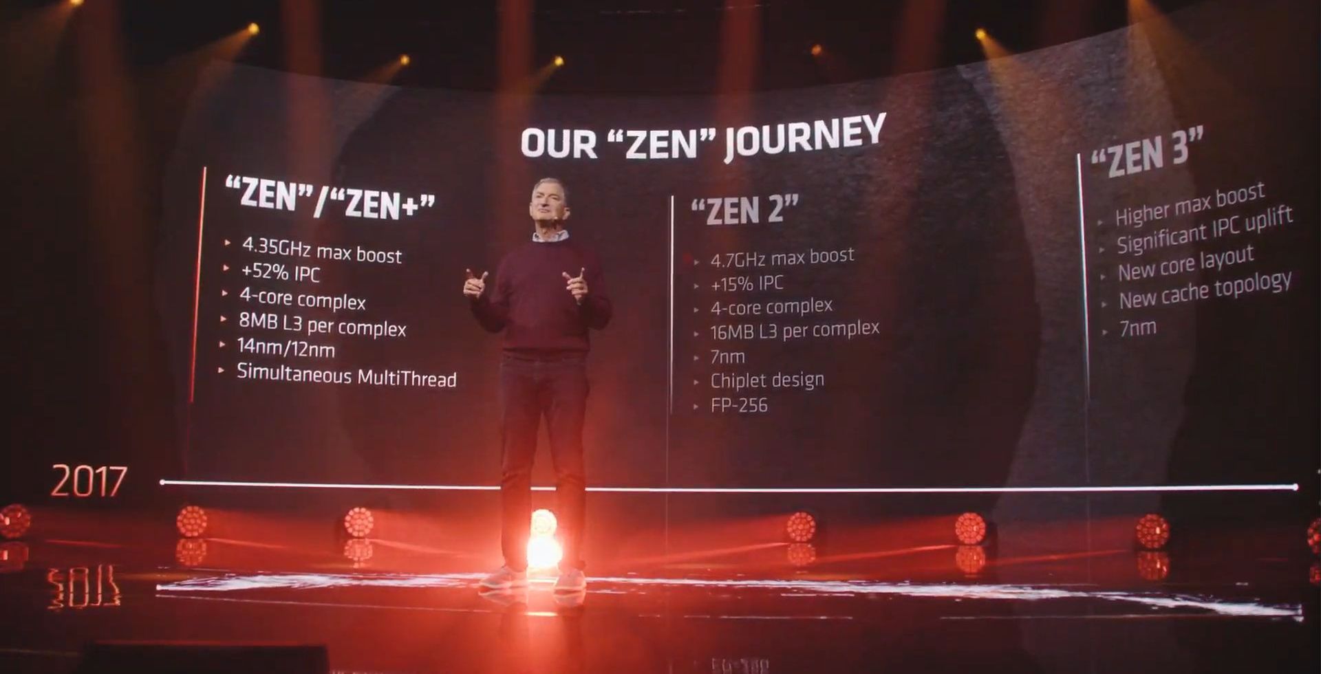
MP: Of our team we are very proud - they are one of the most innovative engineering teams in the industry. So this is a hard fought battle to get into this leadership position with Zen 3 and I can tell you we have a very strong roadmap going forward. The team indeed is staying very very grounded - you look at the kind of approach that we took on Zen 3, and you know it wasn’t any one silver bullet that delivered the performance [uplift], it was really touching almost every unit across the CPU and the team did an excellent job of driving improvements in performance, improvements in efficiency, reducing the latency to memory, and providing a tremendous improvement in performance.
[We achieved] a 19% in a single generation of instruction per clock over our previous generation, which was Zen 2 released just mid of last year. So it was a phenomenal achievement, and it’s that focus on what I’ll call ‘hardcore engineering’ that the team will continue going forward - it won’t be about silver bullets, it will be about continuing to provide real-world performance gains to our customers.
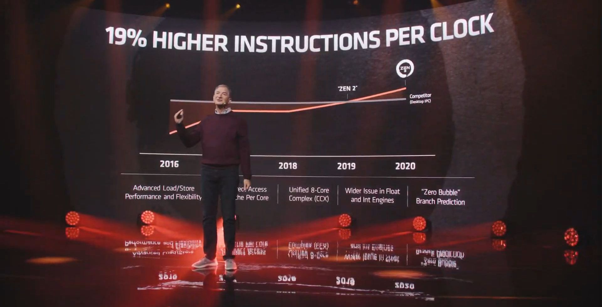
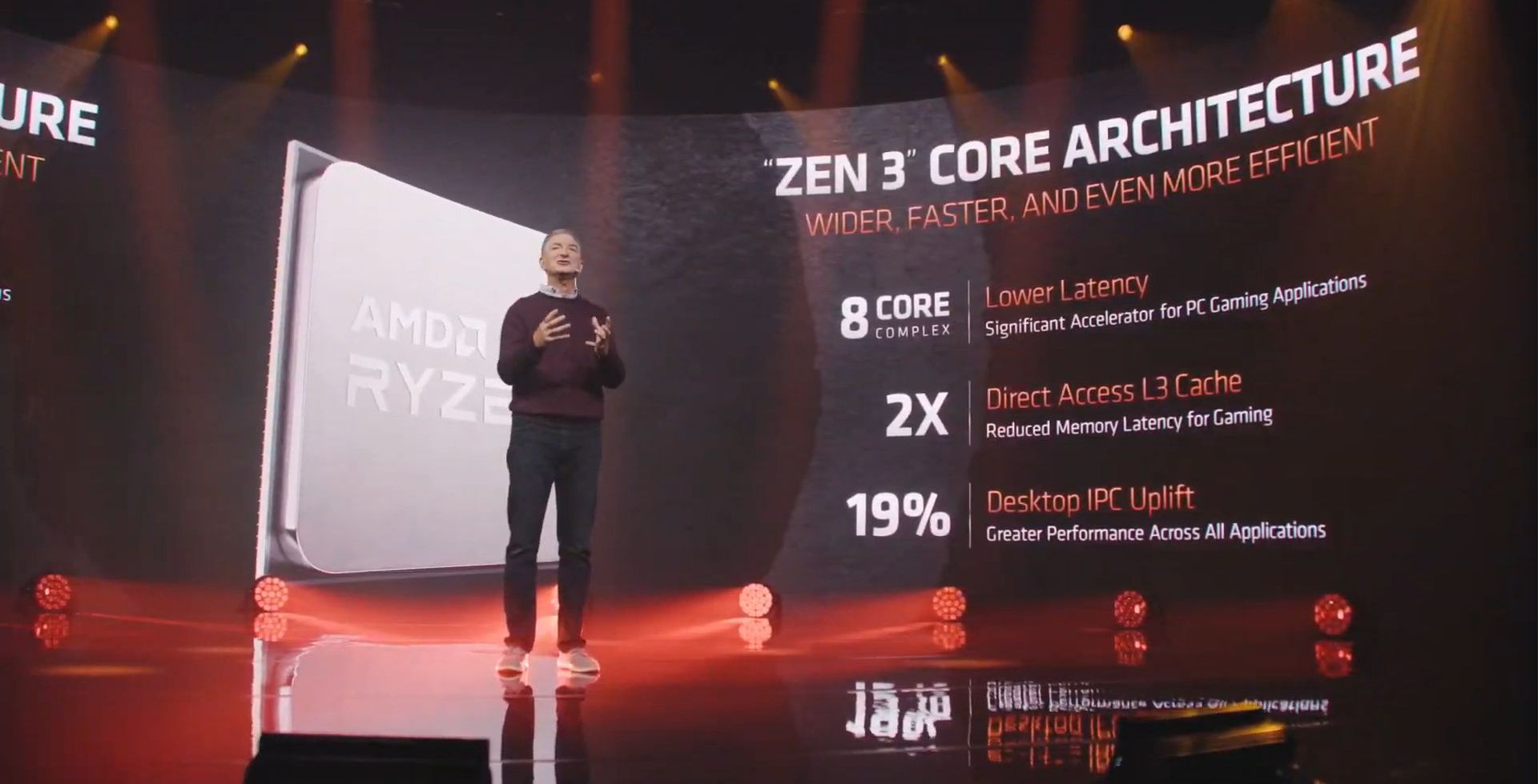
IC: To highlight that 19% value: two of those highlights of AMD’s announcements include the +19% increase in raw performance per clock compared to Zen 2, but also this new core complex design with eight cores and 32 MB of L3 cache. To what extent is the larger core complex helping with the raw performance increase, or are there other substantial benefits in the design by moving to the combined CCX?
MP: The change in the basic construct of the core complex was very very important in allowing us to realize reductions in latency to memory which is huge for gaming. Gaming is a huge market for us in high performance desktop and games typically have a dominant thread - and so that dominant thread, its performance is very dependent on the L3 cache available to it. This is because if it can hit in that local L3 cache, obviously it’s not traversing all the way out to main memory. So by reorganizing our core complex and doubling it to four cores that have direct access to 16 MB L3 cache, by now having eight cores that have direct access to a 32 MB of L3 cache you really - it’s the single biggest lever in reducing latency. Obviously when you hit in the cache you provide effective latency - it directly improves performance. It was a big lever for gaming, but we had a number of levers behind that - again we really touched every unit in the CPU.
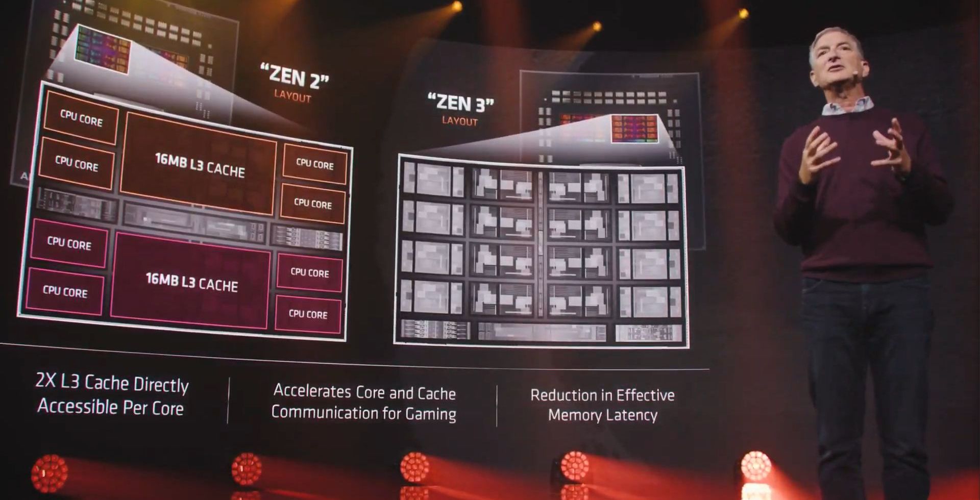
IC: Doubling that L3 cache access for each core, from 16 MB to 32 MB, is a sizable leap I’ll grant you that! It improves that overall latency up to 32 MB as you’ve said so we don’t have to go out to main memory. But has doubling the size affected the L3 latency range at all? Obviously there are tradeoffs when you double an L3 cache, even so when you have more cores accessing it.
MP: The team did an excellent job on engineering, both logically and physically. That’s always the key - how to architect the reorganization, so to change the logic to support this new structure and equally focus on the physical implementation - how do you optimize layout so you’re not adding stages of delay that would effectively neuter the gains? It was tremendous engineering on the reorganization on the Zen 3 core that truly delivers the benefit in reduced latency.
I’ll go beyond that - as we talk about physical implementation, the normal thinking would be when you add the amount of logic changes that we did to achieve that 19% IPC, normally of course the power envelope would go up. We didn’t change technology nodes - we stayed in 7nm. So I think your readers would have naturally assumed therefore we went up significantly in power but the team did a phenomenal job of managing not just the new core complex but across every aspect of implementation and kept Zen 3 in the power envelope that we had been in Zen 2.
When you look at Ryzen as it goes out, we are able to stay in the same AM4 socket and that same power envelope and yet deliver these very very significant performance gains.
IC: Speaking to that process node, TSMC’s 7nm as you said: we’ve specifically been told that it is this sort of minor process update that was used for Ryzen 3000XT. Are there any additional benefits that Ryzen 5000 is getting through the manufacturing process that perhaps we are not aware of?
MP: It is in fact the core is in the same 7nm node, meaning that the process design kit [the PDK] is the same. So if you look at the transistors, they have the same design guidelines from the fab. What happens of course in any semiconductor fabrication node is that they are able to make adjustments in the manufacturing process so that of course is what they’ve done, for yield improvements and such. For every quarter, the process variation is reduced over time. When you hear ‘minor variations’ of 7nm, that is what is being referred to.
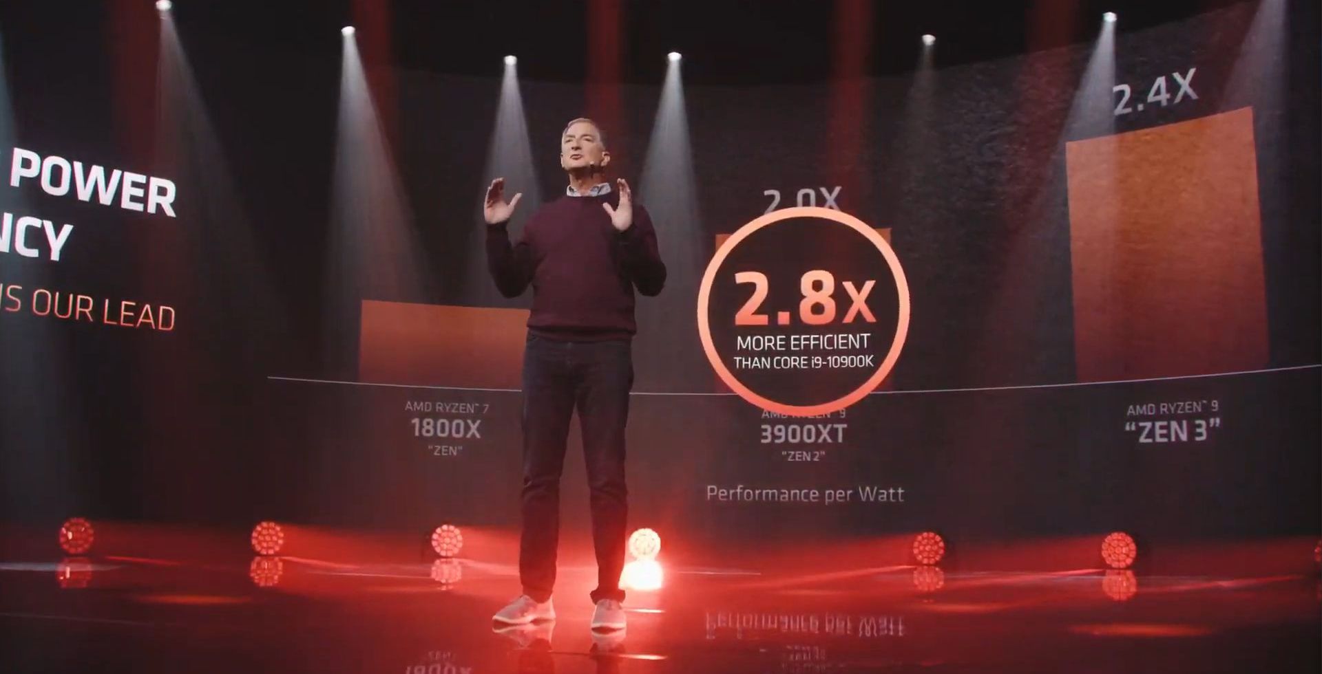
IC: Moving from Zen 2 to Zen 3, the headline number in the improvement of performance per watt is 24% on top of the 19% IPC. This obviously means that there have been additional enhancements made at the power deliver level - can you talk to any of those?
MP: We have a tremendous focus on our power management. We have an entire microcontroller and power management schema that we have across the entire CPU. We enhance that every generation, so we’re very proud of what the Zen 3 team has done to achieve this 24% power improvement. It is yet more advances in whole Precision Boost to give us more granularity in managing both frequency and voltage while constantly listening to the myriad of sensors that we have on the chip. It is yet more granularity and the adaptability of our power management to the workload that our users are running on the microprocessor. So it is more responsive, and being more responsive means that it also delivers more efficiency.
IC: One of the points made on Zen 2 was a relatively high idle power draw of the IO die, anywhere from 13 W to 20 W. We’ve been told that this time around Zen 3 uses the same IO die as Zen 2 did. We just wanted to confirm that does Zen 3 change anything in this regard, given the focus on power efficiency and performance per watt, or is it the same design for the sake of compatibility or cost effectiveness?
MP: These are incremental advancements on the IO die that allowed us to give our customers in high performance desktop, to leverage that AM4 socket while getting these performance gains - that was a very calculated move to deliver CPU performance while giving continuity to our customer base. We are constantly driving power efficiency - with Zen 3 the focus was on the core and the core-cache complex in driving the bulk of our power efficiency.
IC: Can you talk about AMD’s goals with regards to IO and power consumption - we’ve seen AMD deliver PCIe Gen4 in 7nm but the IO die is still based in 12/14nm from Global Foundries. I assume it is a key target for improvements in the future just not this time around?
MP: It’s generational - if you look to the future we drive improvements in every generation. So you will see AMD transition to PCIe Gen 5 and that whole ecosystem. You should expect to hear from us in our next round of generational improvements across both the next-gen core that is in design as well as that next-gen IO and memory controller complex.
IC: Speaking about the chiplet itself, the AMD presentation gave us a high-level view of the increased core complex. We’ve noted that the off-chip communication for those chiplets has now been moved from the center of between the two core complexes to the edge. Are there any specific benefits to this, such as wire latency, or power?
MP: You look at that optimization trade-off, marrying the logical implementation with the physical implementation. So the new cache core complex was designed to minimize latency from the CPU cores themselves into that cache complex. To put the control circuits being placed where they are means the longer wire lengths can go to the less latency sensitive circuits.
IC: Over the last couple of years, AMD has presented that it has a roadmap when it comes to its Infinity Fabric design, such as striving towards the two typical areas of higher bandwidth and better efficiency. Does Zen 3 and the new Ryzen 5000 family have any updates to the IF over Ryzen 3000?
MP: We do - we made improvements, you’ll see new security elements that will be rolling out. We boosted our security, [and] we are always tuning our Infinity Architecture. With Zen 3 the focus was on delivering the raw CPU performance. So in terms of our Infinity Architecture for Ryzen desktop it’s incremental, and we’ll be rolling out some of those details - we’ve very excited about it and it’s a great compliment to the main headline story, which is CPU performance leadership.
IC: With AMD and Intel, we’re now seeing both companies binning the silicon from the fabs to within an inch of its maximum - leaving very little overclocking headroom just so users have that peak performance straight out of the box. From your perspective how do features such as the Precision Boost Overdrive, where frequencies go above the stated range on the box - how do features like that evolve or do they just slowly disappear as binning optimization and knowledge increases over time?
MP: Of course our goal is to maximize what we support with our maximum boost frequency. With Zen 3 we do increase that to 4.9 GHz. We’re always focused on improving our binning - the way you should think about it is [that] we’ll always have the best boost frequency that we can provide, and it is tested across the full gamut of workloads. Our test suite tries to cover literally every type of workload that we believe our customers would be able to run on our CPU. But end-users are very smart, and they might have a segment of those applications, and our thought is that we will continue to provide overclocking so that the enthusiast that really understands their workloads and may have a workload that gives them an opportunity to run even faster given the unique nature of what they are interested in, of what they’re running, and we want to give them that flexibility.
IC: We’ve touched upon security as it relates to changes in the Infinity Fabric - can you comment on AMD’s approaches to the major topics of security vulnerabilities, and if there are any new features inside Zen 3 or Ryzen 5000 to assist with this?
MP: We’ll be rolling out more details on this, but it will continue the train we’ve been on. We’ve always been a security first approach to our design - we’re very very resilient to side channel attacks just based on the nature of our microarchitectural implementation, [and] the way we implemented x86 was very very strong. We have had great success and uptake of the encryption capability we have both across our whole memory space or our ability to encrypt unique instances of virtualization.
We’ll continue that track with Zen 3. We will have more details forthcoming in the coming weeks, but what you’ll see is more enhancements that further protect against other rogue elements out there like Return Oriented Programming (ROP) and other facets that you have seen bad actors try to take advantage of out there in the industry.
IC: Would you say the focus of those security enhancements is necessarily towards the enterprise rather than the consumer, just due to the different environments? Does AMD approach the markets separately, or is it more of a blanket approach?
MP: We generally try and think about what is the best security we can provide across the full array of end applications. Of course, Enterprise is typically will have a higher focus on security, but I believe that has changed over time and everyone, whether you are running your CPU in a high performance application such as content creation, computation, gaming - I believe that security is foundational. So although historically it has been the focus of Enterprise, and it drives our approach of rolling out security enhancements as best we can across all of our products. We believe it is foundational.
IC: Back to the 19% IPC uplift – in part of the presentation, AMD breaks down where it believes those separate percentages come from with different elements of the microarchitecture. It is clear that the updates to the load/store units and the front end contribute perhaps half of that benefit, with micro-op cache updates and prefetcher updates in the other half. Can you go into some slight detail about what has changed in load/store and front-end - I know you’re planning to do a deeper dive of the microarchitecture as we get closer to launch, but is there anything you can say, just to give us a teaser?
MP: The load/store enhancements were extensive, and it is highly impactful in its role it plays in delivering the 19% IPC. It’s really about the throughput that we can bring into our execution units. So when we widen our execution units and we widen the issue rate into our execution units it is one of the key levers that we can bring to bear. So what you’ll see as we roll out details that we have increased our throughput on both loads per cycle and stores per cycle, and again we’ll be having more details coming shortly.
IC: Obviously the wider you make a processor you start looking at a higher static power and active power - is this spending more focus on the physical design to keep the power down?
MP: It’s that combination of physical design and logic design. What I think many people might miss in the story of Zen 3 as we roll it out, the beauty of this design is in fact the balance of bringing extensive changes to drive up the performance while increasing the power management controls and the physical implementation to allow the same typical power switching per cycle as we had in the previous generation - that’s quite a feat.
IC: Zen 3 is now the third major microarchitectural iteration of the Zen family, and we have seen roadmaps that talk about Zen 4, and potentially even Zen 5. Jim Keller has famously said that iterating on a design is key to getting that low hanging fruit, but at some point you have to start from scratch on the base design. Given the timeline from Bulldozer to Zen, and now we are 3-4 years into Zen and the third generation. Can you discuss how AMD approaches these next iterations of Zen while also thinking about that the next big ground-up redesign?
MP: Zen 3 is in fact that redesign. It is part of the Zen family, so we didn’t change, I’ll call it, the implementation approach at 100000 feet. If you were flying over the landscape you can say we’re still in the same territory, but as you drop down as you look at the implementation and literally across all of our execution units, Zen 3 is not a derivative design. Zen 3 is redesigned to deliver maximum performance gain while staying in the same semiconductor node as its predecessor.
IC: While the x86 market for both client and enterprise is very competitive, there is increasing pressure from the Arm ecosystem in both markets, it’s hard to deny. At present, Arm’s own Neoverse V1 designs are promising a near-x86 level of IPC, and subsequent 30% year-on-year architectural uplift, at a fraction of the power that x86 runs at. While AMD’s goals so far have been achieving peak performance, like in Zen 3, but how does AMD intend to combat non x86 competition, especially as they are starting to promise in their roadmaps more and more performance?
MP: We won’t let our foot of the gas pedal in terms of performance. It’s not about ISA (instruction set architecture) - in any ISA once you set your sight on high performance you’re going to be adding transistors to be able to achieve that performance. There are some differences between one ISA and another, but that’s not fundamental - we chose x86 for our designs because of the vast software install base, the vast toolchain out there, and so it is x86 that we chose to optimize for performance. That gives us the fastest path to adoption in the industry. We have historically have lived in nothing but a competitive environment - we don’t expect that to change going forward. Our view is very simply that the best defense is in fact a strong offence - we’re not letting up!

IC: With the (massive) raw performance increases in Zen 3, there hasn’t been much talk on how AMD is approaching CPU-based AI acceleration. Is it a case of simply having all these cores and the strong floating point performance, or is there scope for on-die acceleration or optimized instructions?
MP: Our focus on Zen 3 has been raw performance - Zen 2 had a number of areas of leadership performance and our goal in transitioning to Zen 3 was to have absolute performance leadership. That’s where we focused on this design - that does include floating point and so with the improvements that we made to the FP and our multiply accumulate units, it’s going to help vector workloads, AI workloads such as inferencing (which often run on the CPU). So we’re going to address a broad swatch all of the workloads. Also we’ve increased frequency which is a tide that, with our max boost frequency, it’s a tide that raises all boats. We’re not announcing a new math format at this time.
IC: Has AMD already prepared accelerated libraries for Zen 3 with regard to AI workloads?
MP: We do - we have math kernel libraries that optimize around Zen 3. That will be all part of the roll-out as the year continues.
IC: Moving to competitive analysis, has the nature or approach of AMD’s competitive analysis changed since the first generation of Zen to where we sit today and where AMD is going forward?
MP: We have consistently kept a clear focus on the competition. We look across our x86 competitors, and any emerging competitors using alternate ISAs. No change - one thing that we believe is you always have to do two things. One, listen to your customers, and understand where their workloads are going, where needs may be evolving over time, and secondly, and keep a constant eye on the competition. That is a key part of what got us to the leadership position with Zen 3, and an element of our CPU design culture that will not change going forward.
IC: A lot of success of Zen 2 and both Ryzen and EPYC has been the chiplet approach: tiny chiplets, high yield, and can also be binned for frequency very well. However we’re starting to see large monolithic silicon being produced at TSMC now at 7nm, with some of TSMC’s customers going beyond the 600mm2 range. AMD is in a position now where revenues are growing, market share is growing, and now it comes out with Ryzen 5000 - where do AMD’s thoughts lie on producing CPU core chiplets on a larger scale - obviously [as core counts increase] you can’t end up with a million chiplets on a package!
MP: We innovated in the industry on chiplets and as you saw last year as we rolled out our Zen 2 based products in both high-performance desktop and server, it gave us tremendous flexibility - it allowed us to be very very early in the 7nm node and achieve many manufacturing efficiencies but also design flexibilities. It is that flexibility going forward that you’ll to continue to see drive more adoption of chiplets. We will continue at AMD, and although some of our competitors derided us at our first release of chiplets, frankly you see most of them adopting this approach.
It’s never going to be one size fits all, so I do believe, based on the market that you’re attacking and the type of interaction you have across CPU, GPU, and other accelerators will command whether the best approach is in fact a chiplet or monolithic. But chiplets are here to stay - they’re here to stay at AMD, and I believe they’re here to stay for the industry.
IC: It’s funny you mention competitors, because recently they announced that they are moving to a very IP-block chiplet design scaling as appropriate. This means chiplets for cores, for graphics, for security, for IO - exactly how far down the chiplet rabbit hole to we go here?
MP: There is always a balance - a great idea overused can become a bad idea. It’s really based on each implementation. Everyone in the industry is going to have to find their sweet spot. Of course, there is supply chain complexity that has to be managed - so every design that we do at AMD, we’re focused on how do we get the best performance in the best organization physically, how we implement that performance, and ensure that we can deliver it through our supply chain reliably to our customers. That’s the tradeoff that we make for each and every product architecture.
IC: TSMC recently launched its 3D Fabric branding, covering all aspects of its packaging technology. AMD already implements a ‘simple’ CoWoS-S in a number of products, however (there) are other areas such as TSMC’s chip stacking or package-integrated interposers - I assume that AMD looks at these for consideration into the product stack. Can you talk about how AMD approaches the topic, or what’s being considered?
MP: Our approach to packaging is to partner deeply with the industry - deeply with our foundry partners, deeply with the OSATs. I truly believe that we’re entering a new era of innovation in packaging and interconnect. It’s going to give chip design companies like AMD increasing flexibility going forward. It also creates an environment for increasing collaboration - what you’re seeing is the chiplet technology advance such that you can have more flexibility in co-packaging known good dies. This was always a dream in the industry, and that dream is now becoming reality.
IC: We’ve seen AMD making inroads into other markets where it hasn’t had such a high market share, such as Chromebooks, and AMD’s first generation [Zen] embedded technologies. Does AMD continue to go specifically for these markets, or is there untapped potential in markets in AMD hasn’t particularly played in, such as IoT or Automotive?
[Note this question was asked before the AMD-Xilinx rumors were publicized]
MP: We continue to look at adjacent markets versus where we play in today. We’ve been in embedded, and we are growing share in embedded, so that certainly continues a focus at AMD. What we’re not doing is going after, what I’ll call, the markets that may have a lot of media attention but are not well matched to the kind of high performance and incredible focus that we have at AMD. We want to deliver high performance at a value to the industry, and so we will continue to putting our energies into our share in those that markets that really value what we can bring to the table.
Many thanks to Mark and his team for their time.


202 Comments
View All Comments
deltaFx2 - Wednesday, October 21, 2020 - link
"uOP caches are a hack. They work well for loops, but not highly-branchy code."That's not true at all. The uop cache is a decoded instruction cache. It basically translates variable length x86 instructions to fixed length micro-instructions or micro-ops, so that next time around, you need to do less work to decode it so you can supply more instructions/cycle with a much shorter pipeline. The hard part of x86 is not the number of instructions (even arm has thousands) but the fact that it has variable length, prefixes, etc. So you can think of it as a copy of the instruction cache if you like. Caches naturally cache repetitive accesses better than random access. If you mean uopcache is bad for large instruction cache footprint workloads, yes, but that's true of the instruction cache as well. Uopcaches cut down the branch mispredict penalty which is one reason ARM uses it, I'd guess. ARM, despite what you might have heard, is not a 'simple' ISA, so it also benefits from the slightly shorter pipeline out of the opcache.
>> Here's an idea: why not use main memory for a uOP cache?
That was transmeta/nvidia denver. Both had binary translators that rewrote x86 to VLIW (transmeta) or ARM -> VLIW ARM (denver). The software+VLIW approach has its drawbacks (predication to achieve the large basic blocks necessary for VLIW to extract parallelism). However, it's certainly possible to rewrite it in uop format and have the CPU suck it up. I've been told doing this in a static binary is hard but might be possible to do the denver thing on an x86 CPU and cut out all the fancy compiler tricks. Not infeasible, but the question always arises if it's just fewer points of failure if you did it in hardware (self modifying code for example. It's a thing for VMs, JITs, etc. That's why ARM now has a coherent I-cache for server CPUs)
>> *sigh* I meant ISA registers, obviously.<snip>
Ok, so x86 32-bit had a problem with 8 arch regs with ax/bx/cx/dx reserved for specific uses. x86-64 largely does away with that although the older forms still exist. A problem with few registers is that you have to spill and fill a lot but it's not as big a deal in x86-64 and newer x86 cpus do memory renaming, which cuts out that latency if it occurs. The argument for many architected registers is strong for in-order cores. For OoO, it's debatable.
>> You don't think it generates more stalls, as well?
No. It generates more pipeline flushes, but they're so rare that it's not worth worrying about. The extra work x86 cores have to do is to wait to make sure that out-of-order loads don't see shared data being written to by another core in the wrong order (TSO). So they're kept around for long enough to make sure this is not the case. It's just bookkeeping. Most of the time, you're not accessing shared data and when you are, another core isn't accessing it most of the time so you toss it away. When it happens, the CPU goes oops, lets flush and try again. ARM claimed to do barrier elision to fix the problem created by weak memory models (DSBs everywhere) and it may be that they are doing the same thing on a smaller scale. I could be wrong though, I haven't seen details.
>> Something else that comes to mind as a bit silly is AVX. Perhaps you'll insist it's trivial, but all the upper-register zeroing in scalar and 128-bit operations seems like wasted effort.
Ah but there's a reason for that. ARM used to not do that in Neon 32-bit and quickly realized it's a bad idea. x86 learned from 16bit that it was a bad idea. Preserving the upper bits when you are only using the lower bits of a register means that you have to merge the results from the previous computation that wrote the full 256bit register (say) and your 64 bit result. It creates false dependencies that hurt performance. Neon-32 bit had similar thing where a register could be accessed as quad, or double hi, double lo, or single 0/1/2/3. It sucks, and in one implementation of ARM (A57?), they stalled dispatch when this happens. Aarch64 zeros out upper bits just like x86-64.
>> I'm not a CPU designer, but you'd do well to remember that the performance of a CPU is the combination of hardware *and* software.
Agreed. I'm saying there's nothing inherently lacking in x86 as an ISA. It's not 'pretty' but neither is C/C++. Python is pretty until you start debugging someone else's code. Arguably neither is linux if you ask the microkernel crowd. But it works well.
mode_13h - Friday, October 23, 2020 - link
First, I'd like to thank you for your time and sharing your insights. Also, I have much respect for how long Intel and AMD have kept x86 CPUs dominant. Further, I acknowledge that you might indeed be right about everything you claim.> The uop cache is a decoded instruction cache.
I understand what they are and why they exist. It's probably an overstatement to call them a hack, but my point is that (like pretty much all caches) rather than truly solving a problem in every case, they are an optimization of most cases, at the expense of (hopefully) a few. Even with branch-prediction and prefetching, you still have additional area and power overhead, so there's no free lunch.
> ARM, despite what you might have heard, is not a 'simple' ISA
As I'm sure you know, ARM isn't only one thing. ARMv8-A does away with much of the legacy features from ARMv7-A. Not much is yet known about ARMv9. Of course, ARMv8-A is probably going to be the baseline that all ARM-based servers and notebooks will always have to support.
> That was transmeta/nvidia denver. Both had binary translators that rewrote x86 to VLIW
So, the problem with those examples is that you have all the downsides of VLIW clouding the picture. Nvidia's use of VLIW is the most puzzling, since it really only excels on DSP-type workloads that are much better suited to the GPUs they integrated in the same SoC!
Interestingly, I guess what I was talking about is somewhere in between that and Itanium, which had a hardware x86 decoder. Of course, we know all too well about Itanic's tragic fate, but I was bemused to realize that I'd partially and unintentionally retread that path. And I still wonder if EPIC didn't have some untapped potential, like if they'd added OoO (which is actually possible, with it not being true VLIW). Late in its life, the product line really suffered from the lack of any vector instructions.
> ARM used to not do that in Neon 32-bit and quickly realized it's a bad idea.
SSE also seems to leave the upper elements unchanged, for scalar operations. My concern is that zeroing 224 bits (in case of AVX) or 480 bits (for AVX-512) will impart a slight but measurable cost on the energy-efficiency of scalar operations.
Finally, I should say that this has been one of the best and most enlightening exchanges I've had on this or probably any internet forum. So, I thank you for your patience with my thoughts & opinions, as well as with the 1990's-era commenting system.
deltaFx2 - Saturday, October 24, 2020 - link
Eh, this isn't about whether x86 designers are good or not. My point was that there wasn't anything inherent in the arm isa that made it power or area efficient, but implementation choices by arm to achieve that. Not sure why it bothers me, but this canard about ISAs making a significant difference to power has to die and it just doesn't.>> ARMv8-A does away with much of the legacy features from ARMv7-A.
Aarch64 is not simple. The RISC-V folks called ARM Ciscy in some paper (can't find it; you'll have to take my word for it. They said something to the effect of look how CISCy arm can be). RISC has morphed to mean whatever people want it to mean but originally it was about eschewing microcode. ARM has microcode. No, not a microcode ROM; that's just one way to implement microcode. Microcode is a translation layer between the ISA and the hardware. RISC philosophy was to expose the microarchitecture in the ISA to software so as to have no microcode (and simple instructions that execute in a single cycle to achieve highly efficient pipelining and 1 instruction per cycle. Cutting out microcode was a way of achieving that).
ARM has common instructions that write 3 GPRs. I don't think x86 has 3 GPR writing instructions (even 2 are rare and are special. 128-bit mul and division, iirc). See LDP with autoincrement where the CPU loads 2 GPRs into memory and increments the base pointer. Common loads (LDR) support autoincrement, so they write two destinations.
ARM has instructions that can be considered load-execute operations (i.e. operations with memory sources/destinations). This was a huge no-no in RISC. Consider LD4 (single structure) which reads a vector from memory and updates a particular vector lane of 4 different registers (say you wanted to update the 3rd element in 4 packed byte vector registers). The most likely implementation is going to be microcoded with operations that load, read-modify-write a register.
See: https://developer.arm.com/docs/ddi0596/f/simd-and-...
There's other weirdness if you look closely... adds with shifts, loads with scaled index, flag registers (oh my!) etc. just like x86 and in some instances more capable than x86. Perfectly fine but the RISC folks get an aneurysm thinking about it. OoO machines I think benefit from having more information sent per instruction rather than less.
What Aarch64 did was to get rid of variable length (thumb/arm32), super-long-microcoded sequences (check out ldmia/stmia/push/pop), predicated instructions, shadow registers and some other stuff I can't remember. They did not make it RISC-y, it very much retained the information density. Now unlike x86, ARM can't add prefixes (yet) so you have only 4 bytes that blow up into thousands of instructions. So while it doesn't have the variable length problem of x86, it does have the 'more work to decode' problem and hence its pipeline is longer than say MIPS. Hence the uopcache for power savings (those 3-dest/2-dest instructions are going to get cracked, so why do it over and over?).
>> Nvidia's use of VLIW is the most puzzling,
Nvidia hired the same transmeta people. If you have a hammer, every problem looks like a nail. Also, some people are like the monty python black knight 'tis only a flesh wound'. In fairness, they wanted to do x86 and that needs a license from Intel (not happening) but binary translation would work. I have no idea why VLIW was chosen again. I had heard around the same time, intel was looking into x86->x86 binary translation to help Atom. Probably went nowhere.
>> we know all too well about Itanic's tragic fate,
Tragic is not the adjective I'd choose. Itanium not only sank but dragged a bunch of other viable ISAs with it (PA-RISC, Alpha, possibly even SPARC as Sun considered switching to itanum, IIRC). Itanium should've been torpedoed before it left the harbour. It belongs to the same school of thinking (hopefully dead but who knows) that all problems in hardware can be solved by exporting it to software. RISC was that (branch delay slots, anyone?), VLIW was that, Itanium was that (see ALAT). If only compilers would do our bidding. And maybe they do in 80% of the cases, but it's the 20% that gets you. Itanium has 128 architectural registers plus some predicated registers. Going out-of-order would be impossible. Too many to rename, needs an enormous RAT, PRF, etc while x86 would match it with fewer resources. They went too far down the compiler route to be able to back off.
You're right about SSE. I forgot. Nice discussing this with you too; one often gets zealots on forums like this so its a welcome change. Hope it helped.
mode_13h - Sunday, October 25, 2020 - link
> this canard about ISAs making a significant difference to power has to die and it just doesn't.You make compelling points, but somehow it's not enough for me.
An interesting experiment would be to rig a compiler to use a reduced set of GP registers and look at the impact it has on the benchmarks of a couple leading ARM core designs. That should be trivial, for someone who knows the right parts of LLVM or GCC.
I don't know of an easy way to isolate the rest. Maybe a benchmark designed to stress-test the memory-ordering guarantees of x86 could at least put an upper bound on its performance impact. But, the rest of the points would seem to require detailed metrics on area, power-dissipation, critical path, etc. that only the CPU designers probably have access to.
> Aarch64 is not simple. The RISC-V folks called ARM Ciscy in some paper
Thanks for the very enlightening details. I don't have much to say about this subject, and it seems to me that many discussions about ISAs and uArchs veer off into unproductive debates about orthodoxies and semantics.
Again, I appreciate your specific examples, and many of us probably learned a few things, there. I definitely see the relevance to my earlier speculation about decoding cost.
> OoO machines I think benefit from having more information sent per instruction rather than less.
If information-density is the issue, is it not solvable by a simple compression format that can be decoded during i-cache fills? Perhaps it would be smaller and more energy-efficient than adding complexity to the decoder, and not add much latency in comparison with an i-cache miss.
> Itanium not only sank but dragged a bunch of other viable ISAs
We can agree that the outcome was tragic. At the time, I very much drank the EPIC cool-aide, but I was also programming VLIW DSPs and very impressed with the performance. One explanation I heard of its failure is that Intel's legal team had patented so much around it that an unlicensed competing implementation was impossible, and big customers & ISVs were therefore wary of vendor lock-in.
> It belongs to the same school of thinking (hopefully dead but who knows) that all problems in hardware can be solved by exporting it to software.
As for the school of thought being dead, this is worth a look (with a number of the more interesting details hiding in the comments thread):
https://www.anandtech.com/show/15823/russias-elbru...
Also this comes to mind:
https://www.anandtech.com/show/10025/examining-sof...
I'd imagine Google would somehow be involved in the next iteration of software-heavy ISAs.
> Itanium has 128 architectural registers plus some predicated registers. Going out-of-order would be impossible.
At the ISA level, my understanding is that EPIC allows for OoO and speculative execution - all the compiler does is make the data-dependencies explicit, leaving the hardware to do the scheduling (which is required for binary backwards-compatibility). Also, I'm not clear why they'd require renaming for smaller levels of OoO - it seems to me more an issue in cases of extensive reordering, or for speculative execution. Perhaps the compiler would need to encode an additional set of dependencies on availability of the destination registers?
> You're right about SSE.
Something about the way AVX shoehorns scalar arithmetic into those enormous vector registers just feels inefficient.
deltaFx2 - Thursday, October 29, 2020 - link
Here's a datapoint: Rome 64c@225W or 3.4W per core (SMT on, mind you). Ampere Altra, 80c @250W (3.3GHz SKU), 3.1W. Ampere claims this SKU performs the same as Rome. https://www.servethehome.com/ampere-altra-80-arm-c... , https://www.servethehome.com/ampere-altra-max-targ...Rome will struggle, I expect, at ~100W TDP due to the MCM design (inefficient). However, from a TCO standpoint, high performance at (reasonably) higher power generally wins because of consolidation effects (fewer racks and what not for same throughput). Unless you are power constrained. Anyway, I'll leave it at that.
>If information-density is the issue, is it not solvable by a simple compression format that can be decoded during i-cache fills?
Let's say you have a jump to target 0xFEED for the first time. How would you find the target instruction if it were compressed? You'd need some large table to tell you where to find it and someone would have to be responsible for maintaining it (like the OS, because otherwise it's a security issue). And for large I-cache footprint workloads, this could happen often enough that it would make things worse.
The ideal ISA would be one that studies the frequencies of various instructions and huffman-encodes them down for Icache density. ISAs are never designed that way, though.
The fundamental problem with compiler based solutions to OoO are that they cannot deal with unpredictable latencies. Cache latency is the most common case. OoO machines deal with them fine. Nvidia's denver was particularly strange in that regard as they should have known why transmeta didn't work out and went with the same solution without addressing that problem (static scheduling can't solve that problem. Oracle prefetching can, but it doesn't exist yet)
VISC: Pay attention to the operating frequency in addition to IPC. If you run your machine at 200MHz, for example, you can get spectacular IPC because memory latency is (almost) constant and your main memory is only (say) 20 cycles away instead of 200 cycles away. The artcle says their prototype was 500MHz. Intel acquired them for next to nothing (200Mn?) so it wasn't like they had something extraordinary. Likely an acquihire. Can't say much about Elbrus as I can't tell what they're doing or how well it performs. If I had to bet, I'd bet against it amounting to much. Too much history pointing in the opposite direction.
>> At the ISA level, my understanding is that EPIC allows for OoO and speculative execution -
Oh yeah, you can probably do OoO on VLIW ISAs too. I'm saying, it has too many architected registers. You can solve it by having a backing store for the architectural registers and copying things into the main PRF when needed for OoO execution and all but it's not efficient and will be trounced by an x86 or arm design. EPIC only made sense if it reduced the number of transistors spent on speculative execution and gave that to caches and other things outside the core. Otherwise one might as well stick to an ISA with a large install base (x86). As a concept, EPIC was worth a shot (you never know until you try) but HP/Intel should've known well in advance that this won't pan out and killed it. Intel wanted to get in on big-iron and thought itanium was the ticket, plus it didn't have to compete with AMD and Cyrix and whoever else was around then in x86.
mode_13h - Sunday, November 1, 2020 - link
> How would you find the target instruction if it were compressed?I'm not familiar with the current state of the art, but it does seem to me that you'd need some sort of double-indirection. I'd probably compress each I-Cache line into a packet, and you have some index you can use to locate that, for a given offset.
You could do some optimizations, though. Like, what about having the index store the first line, uncompressed, and then actually encode the location of the next line? That would avoid the latency hit from double-indirection, only adding the overhead of one memory offset, which would be amortized in fetches of subsequent lines. Interleaving offsets in with code (or at least all of the branch targets) would bloat slightly complicate indexing, but I think not much.
> The ideal ISA would be one that studies the frequencies of various instructions and huffman-encodes them down for Icache density.
I know, but if you're only compressing the opcodes, that still won't give you optimal compression.
> The fundamental problem with compiler based solutions to OoO are that they cannot deal with unpredictable latencies.
Yes, we're agreed that some runtime OoO is needed (unless you have a huge amount of SMT, like GPUs). I never meant to suggest otherwise - just that compilers (or their optimizers and instruction schedulers) could play a bigger role.
> Can't say much about Elbrus as I can't tell what they're doing or how well it performs.
If you're interested, check out the comments thread in that article. Some interesting tidbits, in there. Plus, about as much (or maybe even a little less) politics as one would expect.
Thanks, again, for the discussion. Very enlightening for myself and doubtlessly a few others.
mode_13h - Sunday, November 1, 2020 - link
I should add that, as manufacturing process technology runs out of steam, I see it as an inevitability that the industry will turn towards more software-heavy approaches to wring more speed and efficiency out of CPUs. It's mainly a question of exactly what shape it takes, who is involved, and when a level of success is achieved that forces everyone else to follow.deltaFx2 - Tuesday, October 20, 2020 - link
"USB and PCIe aren't x86 standards. " They are Intel IP, standardized. Because unfortunately that's what's needed for wide adoption and intel has a strong not-invented-here culture. There's committees and all that for this but intel is the big dog there. Just like qualcomm is for wireless IP standards. PCIe came about because AMD was pushing non-coherent Hypertransport. So intel decided to nip that in the bud with PCI/PCIe. A long time ago, AMD pushed coherent HT as well, which was adopted by some lke Cray (CXL/CCIX, 20 yrs ago) but AMD's shoddy execution after Barcelona killed it as well. CXL came about because there's no way intel would do CCIX (modified AMBA)Wilco1 - Monday, October 19, 2020 - link
Gaviton 2 is close to the fastest EPYC 7742 on both single-threaded performance and throughput despite running at a much lower frequency. Turning off SMT means losing your main advantage. Without SMT, Rome would barely match Graviton 2. Now how will it look compared to 80 cores in Ampere Altra? Again, how does that make x86 look more competitive?Milan maxes out at 64 cores (you need to redesign the IO die to increase cores, so chiplets are no magic solution) and will still use the basic 7nm process, so doesn't improve much over Rome - rumours say 10-15%.
The facts say 2021 will be the year of the 80-128 core Arm servers. If you believe AMD/Intel can somehow keep up with 64 cores (or less) then that would be fanboyism... DDR5 will help the generation after that and enable even higher core counts (Arm talks about 192 cores using DDR5), but that's going to be 2022.
deltaFx2 - Monday, October 19, 2020 - link
What good is 128 cores if DDR4 bandwidth is insufficient? Niche use cases where data fits in caches?Ampere’s 80 cores “beat” rome in their marketing slides. Where’s the official spec submission? Third party tests? Nope. Can it be produced in volume? If it were, we’d see general availability. A Silicon Valley startup looking for an exit is prone to gross exaggeration.
Rumors are just that. Rumors were that zen 3 had 50% fp ipc uplift. Wait and see.