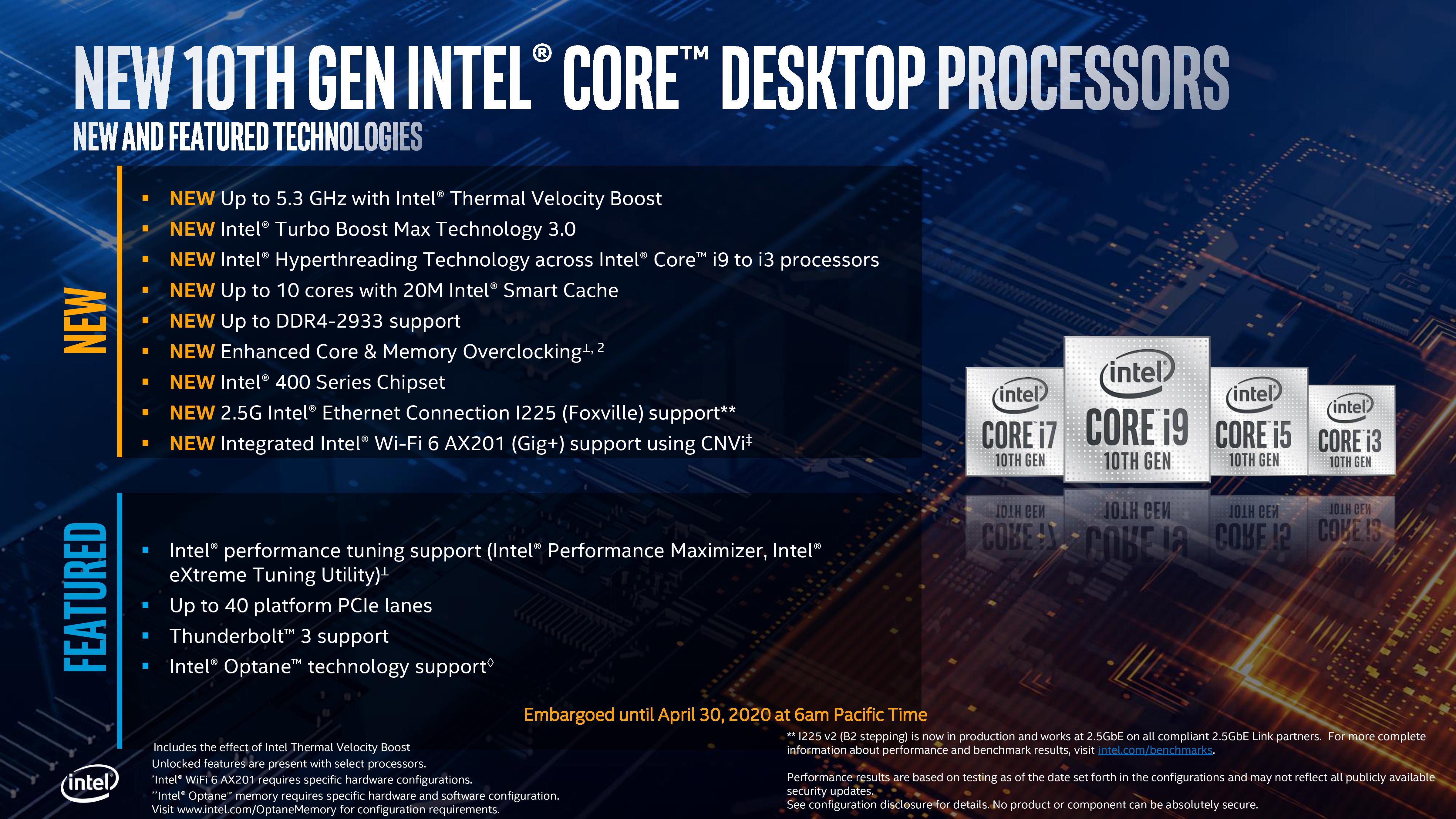
Intel’s 10th Gen Comet Lake for Desktops: Skylake-S Hits 10 Cores and 5.3 GHz
by Dr. Ian Cutress on April 30, 2020 9:00 AM EST- Posted in
- CPUs
- Intel
- Overclocking
- 14++
- Z490
- Comet Lake
- B460
- H470
The Competition
So here’s the big question – how does Intel’s hardware stack up against the Zen 2 processors from AMD. For this, we’re going to do some price-to-price comparisons.
At ~$430, the Core i9-10900F goes up against the R9 3900X
| Battle at ~$430 | ||
| Intel Core i9-10900F |
AnandTech | AMD Ryzen 9 3900X |
| $422 | Price | $432 |
| 14++ | Lithography | 7nm |
| 10C / 20T | Cores | 12C / 24T |
| 2.8 GHz | Base Frequency | 3.6 GHz |
| 65 W | TDP | 105 W |
| 5.1 GHz | Favored Core (TB3) | 4.6 GHz |
| 2 x DDR4-2933 | DRAM Support | 2 x DDR4-3200 |
| PCIe 3.0 x16 | PCIe Support | PCIe 4.0 x24 |
In this instance, Intel has the higher turbo favored core and lower TDP, but AMD has the much higher base frequency, PCIe 4.0 support, and faster memory.
At ~$180, the Core i5-10500 and i5-10400F go up against the popular Ryzen 5 3600:
| Battle at ~$180 | |||
| Intel Core i5-10500 |
Intel Core i5-10400F |
AnandTech | AMD Ryzen 5 3600 |
| $192 | $152 | Price | $173 |
| 14++ | 14++ | Lithography | 7nm |
| 6C / 12T | 6C / 12T | Cores | 6C / 12T |
| 3.1 GHz | 2.9 GHz | Base Frequency | 3.6 GHz |
| 65 W | 65 W | TDP | 65 W |
| 4.5 GHz | 4.3 GHz | Favored Core (TB3) | 4.2 GHz |
| 2x DDR4-2666 | 2x DDR4-2666 | DRAM Support | 2x DDR4-3200 |
| PCIe 3.0 x16 | PCIe 3.0 x16 | PCIe Support | PCIe 4.0 x24 |
The Core i5-10500 has the higher turbo frequency, but don’t forget this is Zen 2 vs Skylake, and Zen 2 has the higher IPC, so that turbo deficit in frequency might actually still be a win for AMD. The fact that the base frequency is in AMD’s favor considerably, plus the DDR4 support and PCIe support, means that the AMD chip is likely the option here. The i5-10400F is in a similar boat, but at least the deficits it does have come with a price reduction.
How about some halo against halo comparison? The Ryzen 9 3950X and 3900X vs the Core i9-10900KF ?
| Halo vs Halo | |||
| Intel Core i9-10900KF |
AnandTech | AMD Ryzen 9 3900X |
AMD Ryzen 9 3950X |
| $472 | Price | $432 | $722 |
| 14++ | Lithography | 7nm | 7nm |
| 10C / 20T | Cores | 12C / 24T | 16C / 32T |
| 3.7 GHz | Base Frequency | 3.8 GHz | 3.5 GHz |
| 125 W | TDP | 105 W | 105 W |
| 5.2 GHz | Favored Core (TB3) | 4.6 GHz | 4.7 GHz |
| 4.8 GHz | All-Core Turbo (TB2) | 4.0 GHz | 3.9 GHz |
| 250-350W ? | All-Core Turbo Power | 136 W | 125 W |
| 2x DDR4-2933 | DRAM Support | 2 x DDR4-3200 | 2 x DDR4-3200 |
| PCIe 3.0 x16 | PCIe Support | PCIe 4.0 x24 | PCIe 4.0 x24 |
Some users will state that the 3900X is the better comparison, only being $40 cheaper, so I’ve included it here as well. Ultimately the thing mainly going for the new hardware is that turbo frequency, up to 5.2 GHz on favored core or 5.3 GHz when under 70ºC. Just looking at the raw CPU data on paper, and some might consider the 10900 series a raw deal.
It should be noted that Intel has different PL2 recommendations for each of the overclockable processors:
- Core i9-10900K: TDP is 125 W, PL2 is 250 W, Tau is 56 seconds
- Core i7-10700K: TDP is 125 W, PL2 is 229 W, Tau is 56 seconds
- Core i5-10600K: TDP is 125 W, PL2 is 182 W, Tau is 56 seconds
Normally the recommended PL2 value is 1.25x the TDP, but in this case Intel is increasing the recommended values. This won’t stop the motherboard manufacturers from completely ignoring them, however.
Also, PL2 and Tau are based on a comparative power load that is defined as a function of a power virus, typically 90-93% or so. This means a complete power virus will go beyond this.
Final Thoughts
Intel is caught between a rock and a hard place. With its main competitor offering sixteen cores on its mainstream platform and on a better process node, Intel’s struggles with its 10nm process means that the company has to rely on old faithful, 14nm, another time. Unfortunately old faithful is showing its age, especially combined with the fifth generation of Skylake, and all Intel can do is apply new optimizations to get the best out of the chip.
This is to be fair, if I was in Intel’s shoes, what I would probably be doing as well. Rearchitecting production lines to start testing for favored cores isn’t as straightforward as users might think, and then adding in more control logic for Thermal Velocity Boost also means expanding out the firmware and driver support too. Adding in things like DMI/PEG overclocking, per-core HT selection, and VF curves, help with keeping the platform interesting.
In an ideal world, on the desktop Intel would be on its second generation of 10nm hardware by now. We would also be on Ice Lake or a post-Ice Lake microarchitecture, and this would be the suitable entry point for PCIe 4.0 connectivity. As it stands we need to wait, and now we have a new motherboard line with partial PCIe 4.0 support for a product that doesn’t exist yet. Unfortunately this is where I think Intel has made its biggest mistake, in having a new socket/chipset combination straddle the generations between PCIe 3.0 and PCIe 4.0. This is going to create a lot of confusion, especially if some of the new motherboards that are designed to meet ‘PCIe 4.0 specification’ end up not working all that well with the future Rocket Lake product. It’s not a hurdle I would like to come across if I was in the target market for this hardware. I would have, if possible, used the previous socket for another generation and then made the change over for PCIe 4.0 and a new socket with Rocket.
While Intel is announcing the hardware, the exact time it will be on shelves is unknown. Typically with these launches we will have a sense of when review samples will be arriving and when the hardware will go on shelves. At this point I still have open questions with Intel as to when that is – I guess that the online retailers will know when their stock is in place and it will be shown on their websites today.


174 Comments
View All Comments
TristanSDX - Friday, May 1, 2020 - link
die size is 200 sqmm. Assuming that Willow Cove core is 2x larger (more cache, AVX512, wider pipeline etc) it is impossible to Rocket Lake have more than 6 coresPeterCollier - Friday, May 1, 2020 - link
Wow, can we get an F in the chat for AMD?Spunjji - Friday, May 1, 2020 - link
Why? 😂twtech - Sunday, May 3, 2020 - link
This is pretty good for a high-end gaming processor, but hardly an overall threat to AMD, who offers better value across their lineup for all uses, and superior processors for laptops, servers, and workstations.abufrejoval - Friday, May 1, 2020 - link
"First up is allowing users to enable/disable hyperthreading on a per-core basis..."Perhaps an overclocker can be forgiven to see the world only in overclocking terms, but these very same chips are also Xeon Es and more so, as core counts increase.
In that context the ability to disable HT on a core-by-core base, ideally even at run-time and in a more fine grained manner might be quite useful for controlling how to deal with VMs running potentially hostile (or sensitve) workloads.
I'm sure Intel doesn't like throwing away HT resources unless it helps salvaging a chip that otherwise would step outside thermal boundries. Yet the side channel leakages potential with HT seems so large, that you can't really afford to leave it on, when dealing with sensitve workloads.
Therefore disabling it on a core-by-core base allows you to pin sensitive VMs to cores without HT, while less exposed back-end workloads can profit from the 10-20% throughput HT may be able to deliver.
Just guessing of course, but generally there has been a trend to expose ever more control about CPU resources (e.g. caches) to hypervisors, to fence anti-social or downright evil workloads.
eastcoast_pete - Friday, May 1, 2020 - link
Wow, all new and improved - packaging! Really?repoman27 - Friday, May 1, 2020 - link
Going by the ordering and spec information listed on ARK, the entire stack is built from two Comet Lake-S dies: the 10-core stepping Q0 and the 6-core stepping G1. They are not using any previous generation Coffee Lake dies or the recently released CML-H 8+2 R1 stepping at this time.Core i5-10600KF and above are Q0 stepping and likely solder TIM.
Core i5-10600 and below are G1 stepping and probably paste TIM (which is fine seeing as they are all locked SKUs with 6 or fewer cores anyway).
Core i5-10400 and Core i5-10400F are the only SKUs that currently list spec numbers for both Q0 and G1 steppings.
Samus - Friday, May 1, 2020 - link
14nm again? I think I just heard Gordon Moore explode.Tchamber - Friday, May 1, 2020 - link
"14nm again?"I was thinking the same thing. I wonder if it's Intel that labels it 14++ or the media. They should have labeled it 14+++++ if it's the 5th iteration.
Fataliity - Saturday, May 2, 2020 - link
:Each plus is a refinement to the 14nm node. Not every 14nm generation from Intel had an improvement to 14nm (They only started this around when Ryzen came into focus and 10nm failed). That's why there are less ++'s than generations of 14nm.