Imagination Announces A-Series GPU Architecture: "Most Important Launch in 15 Years"
by Andrei Frumusanu on December 2, 2019 8:00 PM ESTHyperLane Technology
Another new addition to the A-Series GPU is Imagination's “HyperLane” technology, which promises to vastly expand the flexibility of the architecture in terms of multi-tasking as well as security. Imagination GPUs have had virtualization abilities for some time now, and this had given them an advantage in focus areas such as automotive designs.
The new HyperLane technology is said to be an extension to virtualization, going beyond it in terms of separation of tasks executed by a single GPU.
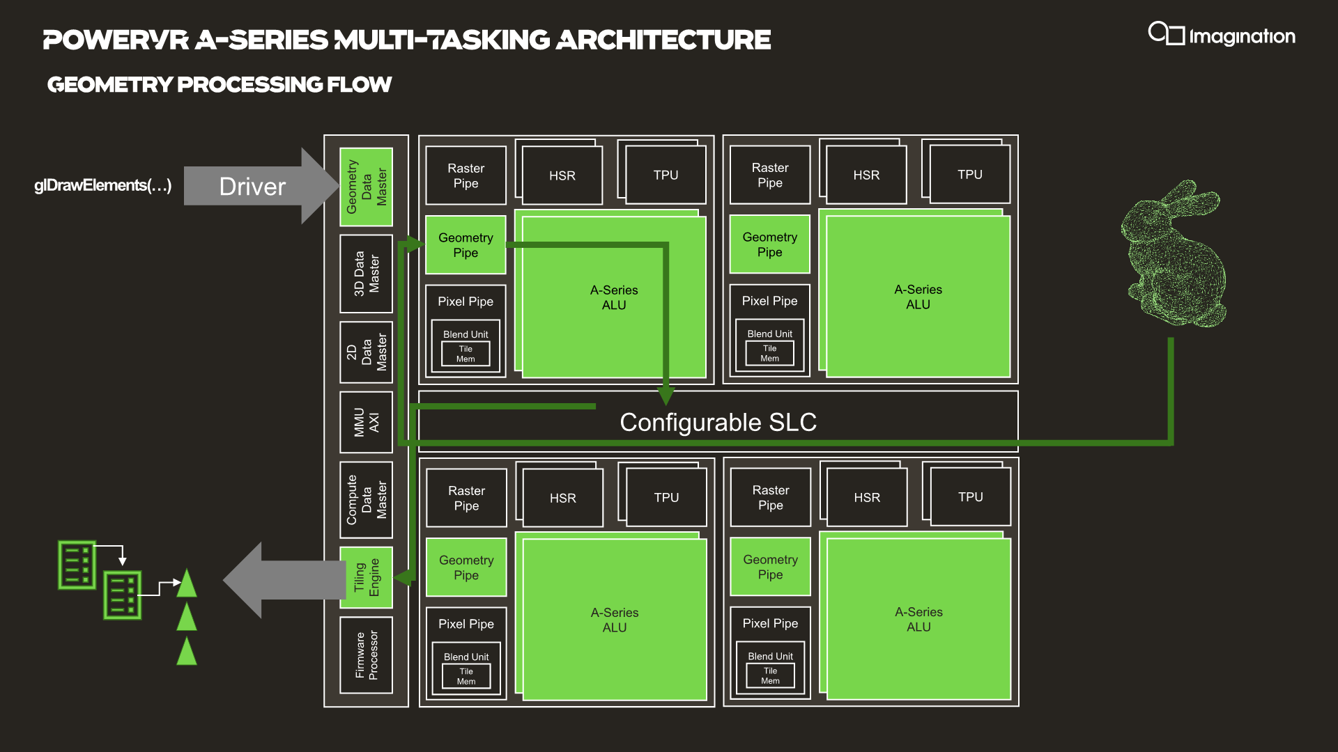
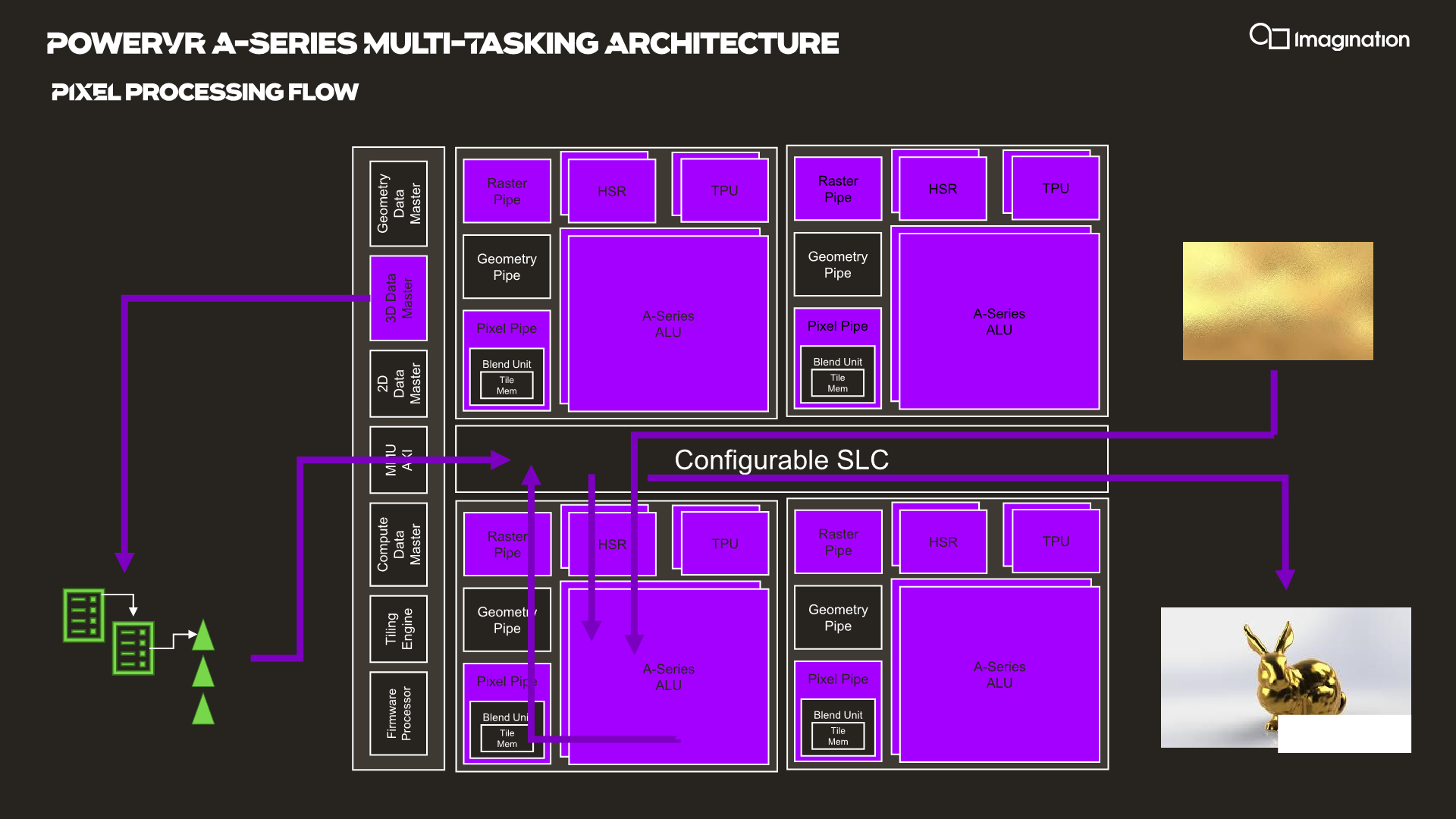
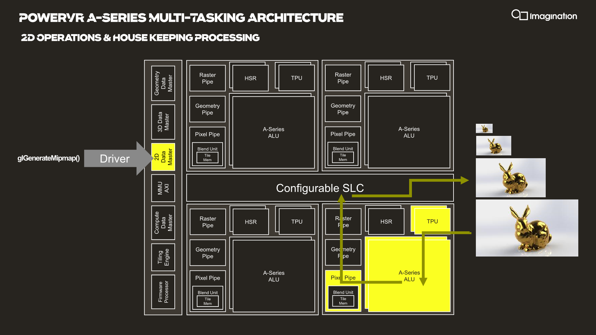
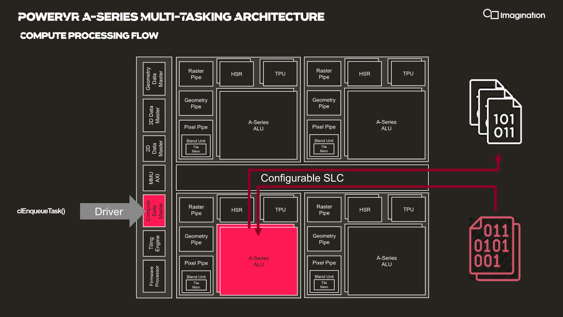
In your usual rendering flows, there are different kinds of “master” controllers each handling the dispatching of workloads to the GPU; geometry is handled by the geometry data master, pixel processing and shading by the 3D data master, 2D operations are handled by the 2D data, master, and compute workloads are processed by the, you guessed it, the compute data master.
In each of these processing flows various blocks of the GPU are active for a given task, while other blocks remain idle.
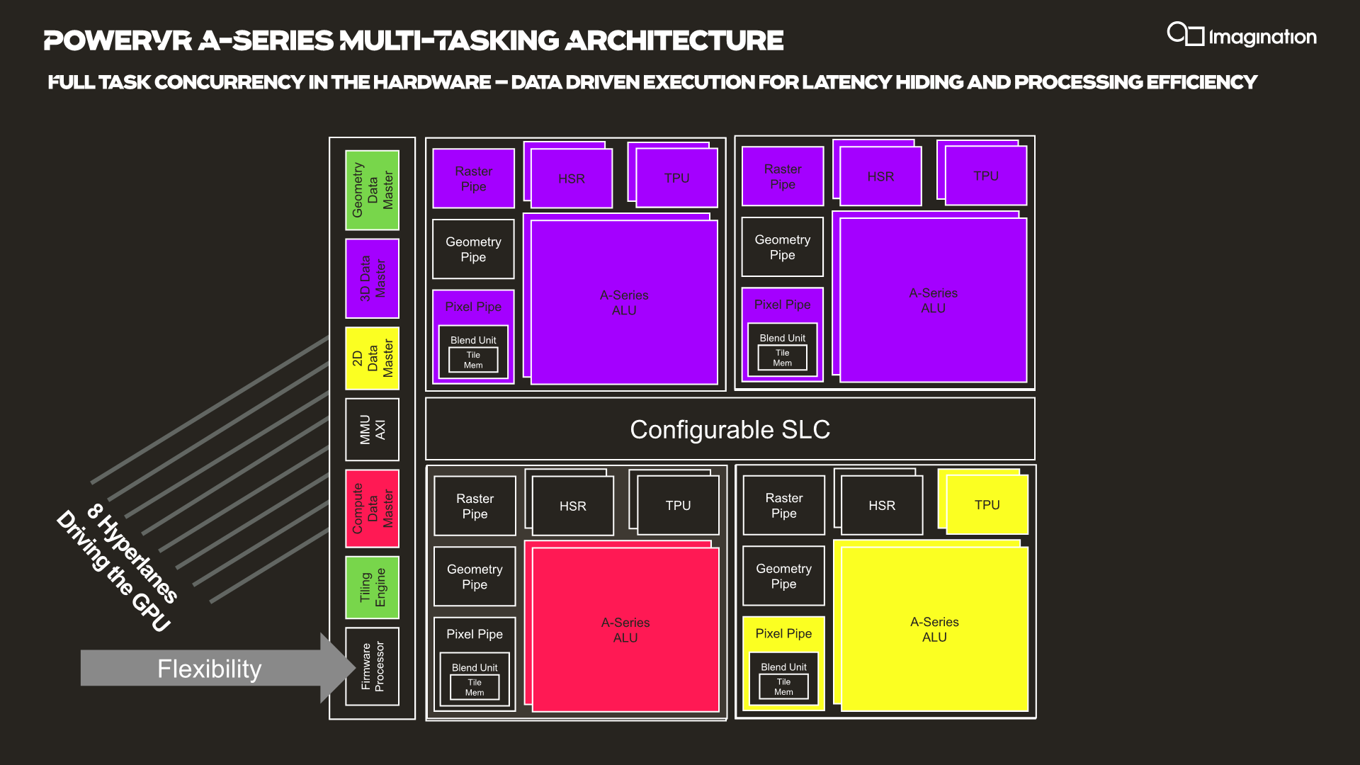
HyperLane technology is said to be able to enable full task concurrency of the GPU hardware, with multiple data masters being able to be active simultaneously, executing work dynamically across the GPU’s hardware resources. In essence, the whole GPU becomes multi-tasking capable, receiving different task submissions from up to 8 sources (hence 8 HyperLanes).
The new feature sounded to me like a hardware based scheduler for task submissions, although when I brought up this description the Imagination spokespeople were rather dismissive of the simplification, saying that HyperLanes go far deeper into the hardware architecture, with for example each HyperLane having being able to be configured with its own virtual memory space (or also sharing arbitrary memory spaces across hyperlanes).
Splitting GPU resources can happens on a block-level concurrently with other tasks, or also be shared in the time-domain with time-slices between HyperLanes. Priority can be given to HyperLanes, such as prioritizing graphics over a possible background AI task using the remaining free resources.
The security advantages of such a technology also seem advanced, with the company use-cases such as isolation for protected content and rights management.
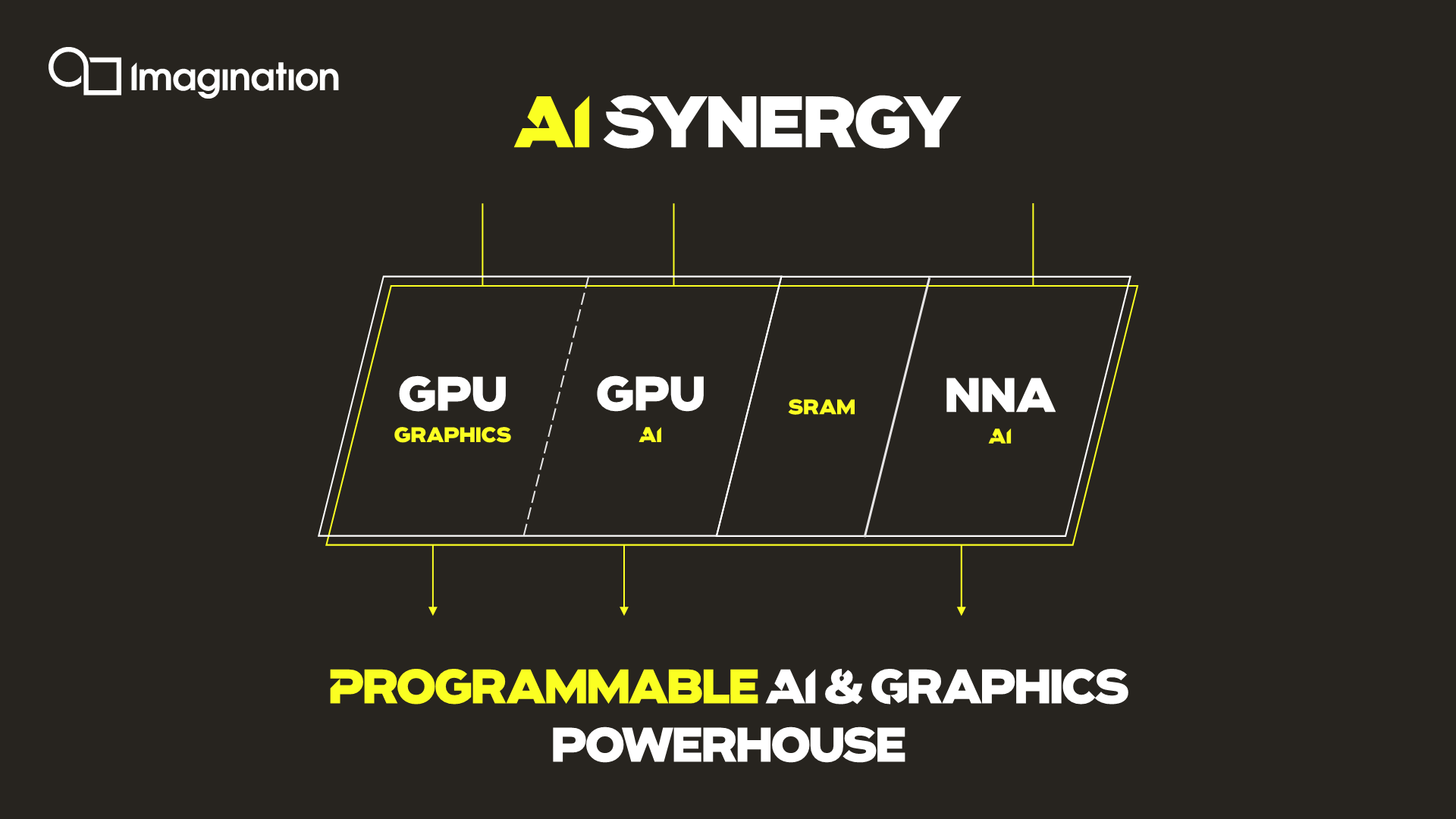
An interesting application of the technology is the synergy it allows between an A-Series GPU and the company’s in-house neural network accelerator IP. It would be able to share AI workloads between the two IP blocks, with the GPU for example handling the more programmable layers of a model while still taking advantage of the NNA’s efficiency for the fixed function fully connected layer processing.
Three Dozen Other Microarchitectural Improvements
The A-Series comes with other numerous microarchitectural advancements that are said to be advantageous to the GPU IP.

One such existing feature is the integration of a small dedicated CPU (which we understand to be RISC-V based) acting as a firmware processor, handling GPU management tasks that in other architectures might be still be handled by drivers on the host system CPU. The firmware processor approach is said to achieve more performant and efficient handling of various housekeeping tasks such as debugging, data logging, GPIO handling and even DVFS algorithms. In contrast as an example, DVFS for Arm Mali GPUs for example is still handled by the kernel GPU driver on the host CPUs.
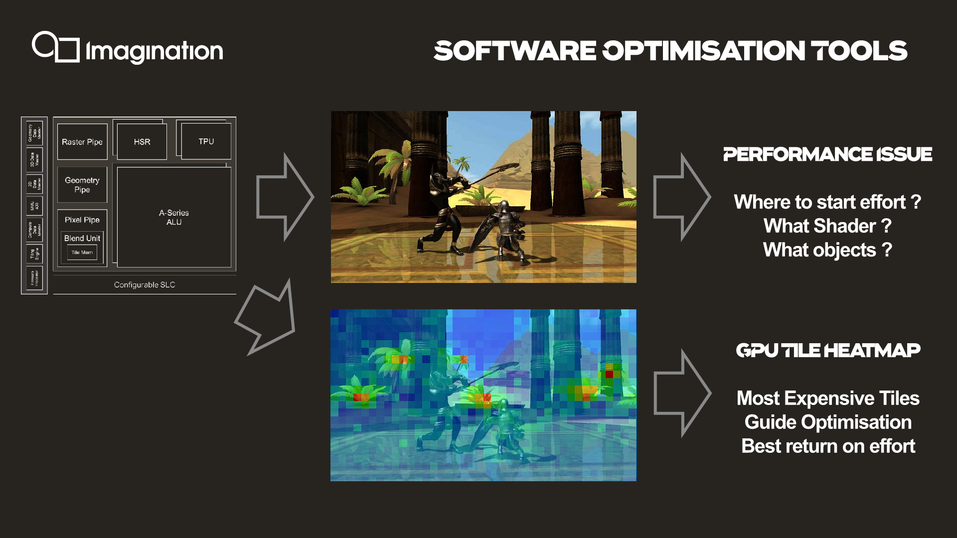
An interesting new development feature that is enabled by profiling the GPU’s hardware counters through the firmware processor is creating tile heatmaps of execution resources used. This seems relatively banal, but isn’t something that’s readily available for software developers and could be extremely useful in terms of quick debugging and optimizations of 3D workloads thanks to a more visual approach.


143 Comments
View All Comments
ET - Tuesday, December 3, 2019 - link
> I fear that this will be a very niche product unless it absolutely dominates all other solutions.At least from the description in the article, it seems to dominate Mali. Even next gen Mali. I don't expect Apple or Qualcomm to move. Samsung I think would be flexible. It's impossible to say how well RDNA fits all price points or when it will arrive, so ImgTech could find a place there. And with the A series supposedly much better than Mali in performance per silicon, I don't think that HiSilicon using it is totally out of the question.
Spunjji - Tuesday, December 3, 2019 - link
No reason HiSilicon can't change their minds if there's a compelling reason. PPA advantages directly translate into cost savings, which is very compelling indeed.MediaTek are probably going to be the biggest customer, though.
mode_13h - Wednesday, December 4, 2019 - link
Chinese want nothing to do with ARM, any more. Got it?So, anyone who's using Mali, or any Chinese phone makers who are using Qualcomm are potential customers.
vladx - Wednesday, December 4, 2019 - link
If you bothered to read the article, you would've found the answer but I guess Americans can't be bothered to read.s.yu - Wednesday, December 4, 2019 - link
"Americans can't be bothered to read"Wow, calling others haters, and look at you.
Etain05 - Tuesday, December 3, 2019 - link
I know that they don’t actually compete, since Apple will never offer its design for licensing, but I still think it’s interesting to compare them.Let’s take the numbers from the Huawei Mate 30 Pro review and compare making some assumptions.
Andrei says: “The comparison implementation here would be an AXT-16-512 implementation running at slightly lower than nominal clock and voltage (in order to match the performance).”
Let’s assume the AXT-16-512 is underclocked by 10% to get to the same performance as the Exynos 9820 and Snapdragon 855. Let’s also assume that an AXT-32-1024 is exactly double the performance of the AXT-16-512.
So, a nominally clocked AXT-16-512 would have 110% the performance of the Snapdragon 855 and Exynos 9820. Double that, and you get 220% the performance, for the AXT-32-1024.
Looking at the Huawei review, here are the numbers:
GFXBench Aztec Ruins High
Exynos 9820 and Snapdragon 855: ~16fps —> AXT-32-1024: 16fps + 120% = 35,2fps
Apple A13: 34fps
GFXBench Aztec Ruins Normal
Exynos 9820 and Snapdragon 855: ~40fps —> AXT-32-1024: 40fps + 120% = 88fps
Apple A13: 91fps
GFXBench Manhattan 3.1
Exynos 9820 and Snapdragon 855: ~69,5fps —> AXT-32-1024: 69,5fps + 120% = 153fps
Apple A13: 123,5fps
GFXBench T-Rex
Exynos 9820 and Snapdragon 855: ~167fps —> AXT-32-1024: 167fps + 120% = 367fps
Apple A13: 329fps
It seems that at least on performance (with generous assumptions), if the new architecture fulfils all promises, it would be competitive, even slightly better than the Apple A13. The problem is that it won’t compete with the A13, but the A14...
How did we get to Apple dominating GPUs too, so fast?
drexnx - Tuesday, December 3, 2019 - link
they're totally unafraid to spend as much die space as they need to get their performance scaling. look at a history of Ax die sizes and you'll see they're all over the placeSpunjji - Tuesday, December 3, 2019 - link
Agreed. It's their vertical integration at work - they're the only company prepared to spend that much die area on performance because they're the only company besides Samsung that can guarantee to sell all every chip they make in a high-end, high-margin device.Andrei Frumusanu - Tuesday, December 3, 2019 - link
Apple's GPUs are the second smallest in the space - only Qualcomm uses less die area.vladx - Wednesday, December 4, 2019 - link
When you extort your customers like Apple does, you can afford to design more expensive SoCs while still keeping huge profits.Apple is the biggest example of what a toxic system capitalism can become.